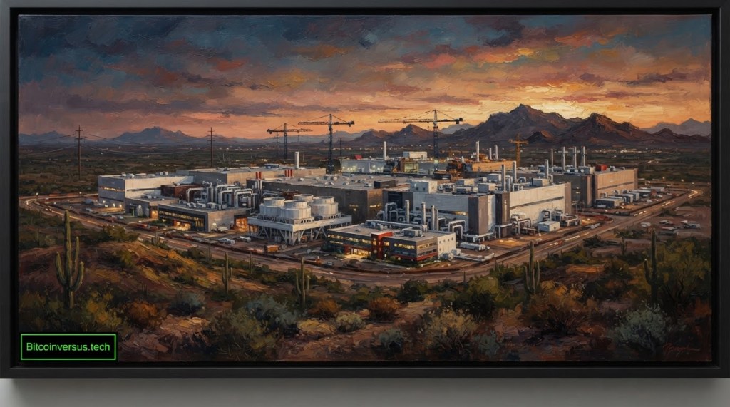
Taiwan Semiconductor Manufacturing Company has expanded its planned Arizona investment to $265 billion, adding another $100 billion commitment announced on July 16, 2026. The expansion is designed to increase U.S. production of advanced chips for artificial intelligence, high-performance computing and mobile devices. The headline number is a long-term capital commitment, not an amount already spent or proof that every proposed factory is operating.
The scale has grown dramatically since TSMC first selected Phoenix in 2020 with an initial $12 billion proposal. Subsequent announcements lifted the commitment to $65 billion and then $165 billion before July’s additional $100 billion. Arizona officials described the latest expansion as four more advanced fabs, while federal officials counted 12 planned semiconductor fabrication and packaging facilities overall. TSMC’s own campus description also identifies a research and development center.
Phoenix Mayor Kate Gallego’s official July 16 announcement on X accompanies the embedded social post. The source link remains accessible when third-party widgets are blocked by browser settings.
TSMC’s first Arizona fab began high-volume manufacturing using its N4 process in the fourth quarter of 2024. The second fab’s building structure was completed in 2025, with N3 volume production targeted for the second half of 2027. The newest expansion targets 2-nanometer and more advanced manufacturing, but a final production schedule depends on customer demand, construction progress and equipment readiness.
Leading-edge chipmaking requires much more than a clean room and lithography tools. A modern fabrication campus depends on reliable electricity, ultrapure water, chemicals, specialty gases, process cooling, wastewater treatment and an extensive supplier network. Lithography patterns circuits onto silicon wafers; deposition, etching, cleaning and inspection repeat across hundreds of manufacturing steps. Packaging then connects finished dies into usable devices, sometimes combining multiple chiplets and high-bandwidth memory.
Arizona’s desert setting adds a major infrastructure challenge. In an official August 2026 video, TSMC said its first fab uses approximately 4.5 million gallons of water daily and that it already reclaims 65% of water. A new industrial water reclamation facility aims to increase reclamation to approximately 90%. Those figures are company statements about its operations and goals, not proof that the entire expanded campus will have negligible water demand.
The investment also has a strategic purpose. TSMC produces advanced chips for major American technology customers, but the company’s manufacturing network remains concentrated in Taiwan. Expanding U.S. production could diversify supply chains and shorten certain logistics routes. It cannot eliminate geopolitical risk, dependence on specialized international equipment, or the difficulty of qualifying advanced processes at new facilities.
Cost is another constraint. Semiconductor fabs are exceptionally capital intensive, and higher construction, labor and operating expenses can affect the economics of U.S. production. TSMC executives have said investment schedules will respond to market conditions and customer demand. The company has not provided a fixed completion date for the entire $265 billion program.
Construction timeline update: Our SmartChart #34 Fab-by-Fab Gantt analysis maps operating production, equipment installation, ongoing construction and forecast milestones across the Arizona campus using dated primary sources.
BitcoinVersus.Tech previously covered TSMC’s Texas discussions, Amkor’s Arizona packaging investment, Fujifilm’s Arizona materials expansion and the semiconductor technician workforce challenge. Together, those developments illustrate why a manufacturing ecosystem needs suppliers, packaging capacity and trained workers alongside wafer fabs.
The essential distinction is between commitment and execution. TSMC’s $265 billion Arizona plan represents an extraordinary expansion of domestic advanced chipmaking capacity, but its ultimate impact will depend on how many facilities reach production, when they do so, and whether demand supports sustained utilization.
Primary documentation
TSMC Arizona project overview; U.S. Department of Commerce announcement; City of Phoenix announcement.


Leave a Reply