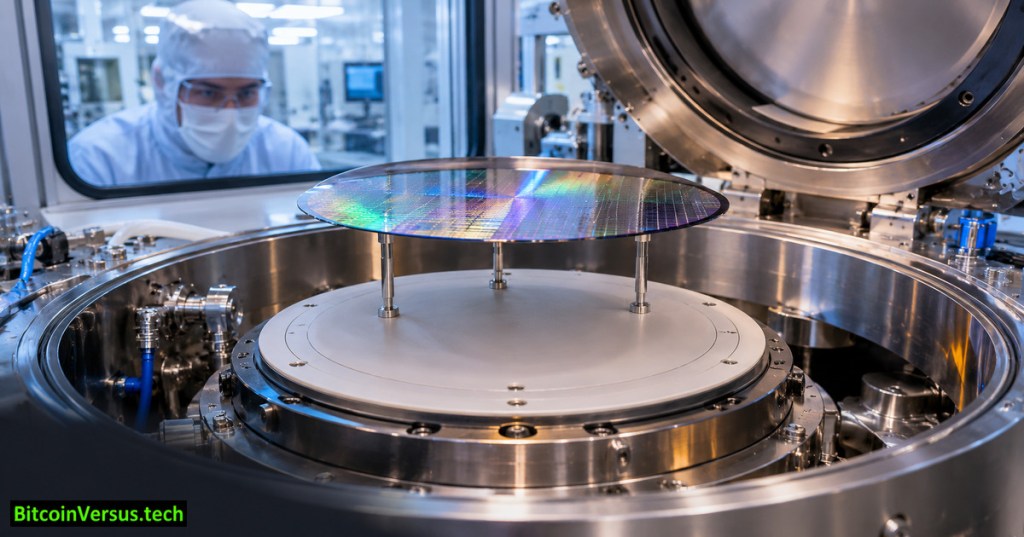
OSSTC.020 follows a silicon wafer after the etch process ends. The chamber has stopped applying the electrostatic chuck’s clamping voltage, yet the wafer may remain attached to its support. Mechanical lift pins can then encounter unexpected resistance. Understanding the difference between turning off a power supply and removing residual holding force is essential for safe wafer handling. The lesson extends OSSTC.019 on backside helium cooling, with a new focus on chuck release, residual electrical charge, and observability.
Learning objectives
- Define electrostatic chucking, dielectric material, residual charge, dechucking, and wafer sticking.
- Compare Coulomb-type and Johnsen–Rahbek-type electrostatic chucks without treating either as a universal design.
- Explain the relationship between electrical discharge, wafer release, and mechanical lift-pin movement.
- Distinguish observable symptoms from demonstrated root causes using a documentation-only example.
- Create a safe, read-only fault-evidence package suitable for equipment-owner escalation.
Prerequisites and scope
Recommended prerequisites are OSSTC.019: Backside Helium Cooling, OSSTC.010: Plasma Etch Basics, and basic ESD and cleanroom handling rules. All activities use fictional records or published evidence. No applied voltage, motion setting, recipe change, chamber opening, or tool access is required.
Elementary overview: how an electrostatic chuck holds a wafer
An electrostatic chuck (ESC) is a wafer-support assembly with embedded electrodes under an electrically insulating or controlled-resistivity surface. A voltage difference establishes an attractive force between the support and wafer. A dielectric is a material that electrically insulates while permitting electric polarization. The ESC may also contain temperature-control elements, backside-gas passages, and access for lift pins. The exact physical construction varies by equipment family.
An ESC can secure a wafer inside a low-pressure plasma chamber without gripping the wafer edge with a conventional mechanical clamp. Once processing ends, dechucking means reducing the holding force enough for a qualified handling mechanism to lift and transfer the wafer safely. A normal ‘voltage off’ indicator does not prove the wafer has been fully released. Surface charge, dielectric polarization, process-dependent electrical conditions, and physical adhesion may persist.
Coulomb and Johnsen–Rahbek holding mechanisms
Two commonly discussed ESC operating regimes are Coulomb-type and Johnsen–Rahbek (J–R)-type. Coulomb-type holding primarily reflects electrostatic attraction across the insulating separation between electrode and wafer. J–R behavior involves a somewhat conductive dielectric and small interfacial contacts, allowing a strong field and additional holding effect near microscopic contact regions. Actual devices can show overlapping behavior, and wafer backside coatings and surface condition matter.
A comparative laboratory study by Gyu Il Shim and Hideo Sugai, published in Plasma and Fusion Research in 2008, observed different discharge-current behavior. Their Coulomb-type test produced a short exponential current decay with a reported 0.14 ms time constant; the J–R setup showed a smaller, longer-lived nonexponential current persisting around 1,000 ms. Those measurements belong to the tested laboratory arrangements, not to a universal wafer-release timer. Read the original study.
The release sequence: electrical and mechanical stages
| Stage | Underlying purpose | Read-only evidence to review |
|---|---|---|
| Clamp | Establish a secure wafer-to-support interface | Clamp state, commanded profile, wafer-present signal |
| Process | Maintain stable support while plasma and thermal systems operate | Recipe phase, alarms, backside helium trend |
| Dechuck command | End the clamp phase and initiate the tool’s approved discharge sequence | Event timestamp, controller phase and completion status |
| Release confirmation | Establish adequate electrical/mechanical conditions for separation | Available charge, capacitance or release-state indicators |
| Lift and transfer | Raise wafer on pins and present it to the transfer mechanism | Lift confirmation, motion or torque alarm, robot-handling event |
Not every chamber exposes each measurement; some estimates are derived internally from controller data. The stages are conceptual, not an authorization to command a sequence. Advanced Energy’s ESC application note discusses clamp/process/de-clamp waveform control and monitoring. The document is a manufacturer’s application note, not a substitute for the site’s current tool manual.
Why a wafer may stick after voltage removal
- Residual electrical charge: charge trapped on wafer surfaces or the chuck’s dielectric can maintain a field after commanded voltage ends.
- Dielectric and interfacial effects: resistivity, contact geometry and J–R behavior influence relaxation and release characteristics.
- Wafer-specific factors: backside films, contamination, bow, temperature and process history can alter contact or charge retention.
- Mechanical factors: a misaligned lift mechanism or debris may resemble electrostatic sticking, so an observed lift fault alone is not proof of residual charge.
- Controller and sensor states: an incomplete or delayed process transition may prevent release even if an operator display appears otherwise normal.
A published U.S. patent describing charge sensing through a lift-pin path provides one example of how wafer-charge information may be obtained in a designed system. A patent describes a technical approach; it does not demonstrate that every fab tool implements the same sensor or control architecture.
Evidence from semiconductor manufacturing research
Researchers at Renesas Semiconductor Manufacturing presented a residual-charge monitoring study at AEC/APC Symposium Asia 2017. The group evaluated a monopolar Coulomb-type ESC on oxide etch equipment, using an electrostatic measurement arrangement to study charge left after chucking and discharge. Their analysis showed that a discharge step that is too brief can leave charge, while an excessively long reverse-voltage application can produce an opposite-polarity charge. Their reported optimum applied to their experimental setup and must not be copied as a recipe parameter.
The lesson’s practical distinction: equipment measurements and qualified engineering trials can establish a cause; a single generic alarm cannot. Historical research helps explain physical mechanisms, while present-day operating limits must come from the relevant approved maintenance instructions.
Practical workflow: read-only evidence gathering
Consider a fictional chamber that records repeated ‘wafer release incomplete’ alarms after a stable production recipe. An authorized technician can assemble a noninvasive evidence package from existing alarms and trend logs. The following checklist does not require opening a chamber, downloading restricted data to personal devices, or changing tool parameters.
- 1. Establish scope: record chamber identifier, alarm time, recipe identifier, wafer lot reference (redacted for training), and the authorized owner of the investigation.
- 2. Verify the sequence: compare process end, clamp-off request, discharge-stage completion, lift authorization, and actual lift-alarm timestamps.
- 3. Compare a baseline: use a known-good wafer or historical run with the same tool, wafer type, recipe and ambient conditions where possible.
- 4. Review correlated channels: examine the existing ESC supply status, wafer-present signal, backside gas control, stage temperature, and lift-pin alarms without changing configuration.
- 5. Separate hypotheses: list evidence supporting residual charge, mechanical interference, wafer backside condition, or incomplete process-state transition. Mark each as unconfirmed until corroborated.
- 6. Escalate: provide the timeline, approved log identifiers, observed deviations, scope, and relevant service manual references to the tool owner or qualified equipment engineer.
Illustrative alarm timeline
| Clock time | Recorded event | Interpretation |
|---|---|---|
| 14:20:00 | Etch process complete | Process phase ended; release not yet proven |
| 14:20:01 | ESC clamp-off command accepted | A command acknowledgement, not a wafer-release measurement |
| 14:20:03 | Lift interlock remains pending | More evidence needed; do not bypass |
| 14:20:05 | Wafer release incomplete alarm | Possible electrical or mechanical condition; cause undetermined |
| 14:20:06 | Transfer inhibited | Safety sequence prevented further motion |
All timestamps, events and outcomes in the table are fictional. No tool was operated or tested for the lesson.
Safety, security, and escalation
ESC systems can combine high voltage, RF energy, vacuum, reactive process gases, stored energy, hot surfaces, and brittle wafers. A technician must never lift a stuck wafer by force, defeat a lift interlock, alter discharge polarity or duration, touch exposed HV connections, or open an inadequately isolated chamber as a classroom exercise. Those actions require the equipment owner’s authorization, manufacturer instructions, qualified personnel, site safety controls, hazard evaluation, lockout/tagout where applicable, and a documented recovery plan.
Wafer fragments create both contamination and injury risks. A failed transfer can also affect robot alignment, hidden wafer mapping and downstream yield. An alarm record can expose proprietary recipes or lot data; share only the minimum information through approved channels. Compare adjacent troubleshooting concepts in OSSTC.013 on chamber particles and OSSTC.016 on vacuum leak detection.
Glossary
- Chucking: holding a wafer against a support through an engineered force.
- Dechucking: controlled reduction of holding force before wafer release.
- Dielectric: insulating material that can store electrical polarization.
- Residual charge: electrical charge remaining after the intended clamping phase.
- Johnsen–Rahbek effect: electrostatic attraction associated with resistive dielectric and microcontact behavior.
- Lift pin: controlled mechanical element used to lift a wafer from a processing stage.
- Interlock: condition or device preventing unsafe or out-of-sequence operation.
Exercises
Exercise 1 (paper-only): Create a two-column comparison of Coulomb and J–R mechanisms, identifying the role of dielectric behavior and why measured release response can differ. State why a single published time constant is not a process setting.
Exercise 2 (paper-only): Read the illustrative alarm timeline. List two observations, two unverified hypotheses, and three pieces of additional evidence needed before a root-cause conclusion.
Exercise 3 (read-only): Using the manufacturer application note and the Renesas study, explain why ‘turn voltage off’ and ‘the wafer can be lifted’ are not equivalent statements. Do not reproduce experimental voltage or time settings as operational recommendations.
Knowledge check with answer key
Q1. Why might a wafer remain held after a clamp-off command? Answer: retained charge, dielectric/interface effects, or process-state issues may prevent sufficient force reduction. A mechanical fault can produce a similar alarm.
Q2. Does a long release delay prove J–R behavior? Answer: No. The type and cause require tool-specific evidence; wafer, mechanical, thermal and electrical conditions can contribute.
Q3. What does an accepted clamp-off command prove? Answer: Only that the controller accepted the command; it does not establish zero residual charge or confirmed release.
Q4. Should a technician bypass a lift interlock to test a sticking hypothesis? Answer: No. Stop and follow the owner-approved escalation procedure.
Exercise 2 sample answer: Observations include clamp-off acknowledgement and an incomplete-release alarm. Hypotheses include residual charge and a mechanical lift condition. Needed evidence could include the full state transition log, matched-run comparison, and any qualified available charge or lift-sensor records.
References and editorial limits
- Shim and Sugai, “Dechuck Operation of Coulomb Type and Johnsen-Rahbek Type,” Plasma and Fusion Research, 2008.
- Advanced Energy, “The Electrostatic Semiconductor Wafer Clamping/Chucking System,” manufacturer application note.
- Hamaguchi et al., Renesas, “The Advanced Monitoring Method for the Residual Charge in Wafer,” AEC/APC Symposium Asia, 2017.
- U.S. Patent 8,111,499 B2: sensing and removing residual charge from a processed wafer.
Media note: The original featured illustration is a conceptual image, not an actual wafer processing record. The saved approved BitcoinVersus.tech tag appears only on the featured cover. No duplicated featured image has been placed inside the article, and no unverified video embed is claimed to play.
We volunteer daily to ensure the credibility of the information on this platform is Verifiably True. If you would like to support to help further secure the integrity of our research initiative, please scan the QR code below.



Leave a Reply