Elementary Overview
SPI engineering is the design of the entire communication path, not just the act of sending bytes. The engineer chooses clock mode, clock frequency, chip-select behavior, word size, transaction boundaries, buffering, DMA strategy, concurrency rules, electrical limits, and recovery behavior so every peripheral remains reliable under worst-case timing and loading.
This lesson follows OSFEC.007: I²C Bus Engineering. It also complements OSFTC.008: SPI Bus Troubleshooting. The technician lesson asks, “Why is this bus failing?” The engineer lesson asks, “How should this bus be designed so it remains correct, scalable, observable, and recoverable?”
SPI Is A De Facto Interface, Not One Universal Protocol
The Linux kernel’s SPI overview describes Serial Peripheral Interface as a synchronous serial link commonly using SCK, MOSI, MISO, and chip select. It also emphasizes that SPI is a de facto interface rather than a single formal standard. That matters because devices can differ in word length, bit order, chip-select timing, half-duplex behavior, daisy chaining, and command framing.
Microchip’s SPI introduction likewise describes one host controlling one or more clients, with the host generating the serial clock and typically assigning a separate select line to each client.
CPOL And CPHA Define The Sampling Contract
Clock polarity, CPOL, defines the idle state of SCK. Clock phase, CPHA, determines whether data is sampled on the first or second active clock edge. Together they produce SPI modes 0 through 3.
- Mode 0: CPOL 0, CPHA 0.
- Mode 1: CPOL 0, CPHA 1.
- Mode 2: CPOL 1, CPHA 0.
- Mode 3: CPOL 1, CPHA 1.
Microchip’s timing documentation shows why “correct mode” is not enough. Setup time, hold time, clock-high and clock-low width, output delay, and signal rise/fall time all consume timing margin.
A host can therefore use the nominally correct mode and still fail at high speed if the client data output becomes valid too late or the PCB, isolator, level shifter, or cable delays the signal into the sampling edge.
DigiKey — STM32 SPI implementation covering bus topology, CPOL/CPHA, logic-analyzer timing, polling, and interrupt-driven transfers.
Timing Margin Is A Budget
For each receive edge, the engineer needs enough time for the transmitter output to change, propagate across the board, pass through any level translation, settle at the receiver, and still satisfy receiver setup time before sampling.
A useful conceptual inequality is:
available half-cycle time > output delay + propagation delay + edge-settling time + setup margin
Do not turn that conceptual relation into a universal numeric formula. The actual timing terms and reference edges come from the host-controller and peripheral datasheets. At higher SCLK rates, a few nanoseconds of added delay can consume a large fraction of the available margin.
Chip Select Is Part Of The Protocol
Chip select does more than identify a peripheral. Many devices define minimum CS-to-clock setup time, clock-to-CS hold time, minimum deselect time between commands, or a requirement that CS remain asserted across command, address, dummy, and data phases.
If software toggles CS between two transfers that the device expects to be one atomic transaction, the peripheral can interpret the second transfer as a new command. This is why high-level driver APIs need a transaction model rather than independent byte writes.
Design Multi-Device Buses Around Per-Device Constraints
Multiple clients can share SCK, MOSI, and MISO while using independent chip-select lines. The design becomes more difficult when the clients require different SPI modes, frequencies, bit orders, word sizes, or CS timing.
Microchip notes that if multiple clients require different CPOL/CPHA settings, the host must reconfigure itself before communicating with the next client. The firmware architecture therefore needs a per-device configuration object rather than one global “SPI setup.”
A representative device descriptor may include mode, maximum SCLK, bits per word, CS polarity, required setup/hold delays, DMA capability, and transaction-specific timeout. The driver should apply those constraints before asserting CS.
Throughput Is Lower Than Raw Clock Rate
An SPI bus clocked at 20 MHz does not automatically deliver 20 Mbit/s of useful application data. Real transactions contain command bytes, addresses, dummy clocks, status reads, chip-select gaps, software latency, and sometimes half-duplex turnaround.
A simple efficiency model is:
payload throughput ≈ SCLK × useful payload bits ÷ total clocked and idle transaction time
Long sequential reads can approach the raw bus rate. Short register transactions may spend more time in command overhead and software setup than transferring payload.
DMA Changes The CPU Cost Of SPI
For long or frequent transfers, pair SPI with the methods from OSFEC.006: Direct Memory Access. DMA can move transmit and receive buffers between memory and the SPI peripheral while the CPU performs other work.
DMA does not make transaction design disappear. The engineer still has to handle buffer ownership, cache coherency where applicable, alignment, completion signaling, errors, timeouts, and chip-select lifetime. A DMA completion interrupt may mean “bytes reached the peripheral FIFO,” “all bits left the shift register,” or something in between depending on the controller.
RTOS Concurrency Needs One Bus Owner At A Time
In an RTOS, several tasks may need the same SPI controller. The scheduling concepts from OSFEC.002 now become bus-design constraints.
Do not let two tasks independently change mode, clock rate, or chip select while another transaction is active. A common architecture uses one SPI service, mutex-protected transaction API, or queued bus worker. Each request carries the target device, buffers, length, deadline, and completion mechanism.
Priority inversion can matter when a high-priority control task waits behind a long low-priority SPI transfer. Engineers may need bounded transfer sizes, priority-aware queues, or separate controllers for time-critical peripherals.
Linux Models SPI As Devices, Messages, And Transfers
The Linux SPI framework separates controller drivers from protocol drivers. A spi_device represents one target device. A spi_message groups one or more spi_transfer operations into an atomic protocol sequence.
That model captures an important engineering idea: command, address, delay, read, and write phases often need to remain one logical transaction. Linux also supports per-transfer delays, CS-change control, synchronous wrappers such as spi_sync(), and asynchronous submission through spi_async(). Controller drivers may use DMA underneath the same protocol interface.
Signal Integrity Limits Practical SCLK
SPI is commonly a short-board interface, but fast edge rates make PCB geometry matter. Problems can include ringing, overshoot, undershoot, crosstalk, ground bounce, reflections, weak return paths, and excessive capacitive loading.
The practical maximum SCLK can therefore be lower than the controller’s advertised maximum. Microchip explicitly notes in one current timing specification that maximum clock frequency can depend on the specific PCB layout.
Series damping resistors near the source are sometimes used to control edge ringing, but values are design-specific. Measure before changing the network. A slower edge with adequate timing margin can be more reliable than an unnecessarily aggressive edge.
Rohde & Schwarz — SPI decode with analog/digital channel assignment, mode settings, thresholds, triggering, and decoded results.
Logic Decode Is Necessary But Analog Evidence Still Matters
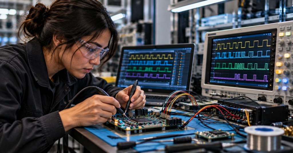
Saleae’s SPI analyzer guide lets engineers configure clock, MOSI, MISO, enable/CS, sampling edge, bit order, and word size. That is ideal for confirming protocol structure.
But a correct decode does not prove robust margin. Inspect the analog waveform when operating near limits. Measure actual SCLK period, clock duty cycle, data setup/hold relative to the receiver edge, CS setup/hold, and logic thresholds under worst-case loading.
Saleae Support — official protocol-analyzer walkthrough showing SPI decode and the effect of sampling-edge configuration.
Saleae’s newer mixed-signal hardware also reflects a broader engineering trend: protocol decode and analog electrical evidence are increasingly being examined together during embedded-system validation.
Saleae community example — mixed-signal bench analysis using modern logic-analyzer/MSO hardware.
Error Handling Must Exist Above The Wires
SPI itself does not provide universal acknowledgement, addressing, CRC, retry, or discovery. Those features belong to the peripheral protocol or application layer. A driver should therefore distinguish bus completion from semantic success.
Examples include verifying JEDEC ID after flash startup, checking a status register after a write, validating a CRC when the device protocol supplies one, confirming a sequence counter, or using a watchdog timeout when the client never becomes ready.
For flash-specific behavior, connect this to OSFTC.007: SPI NOR Flash Diagnostics. For low-level debug, use OSFEC.003: Hardware Debugging with JTAG, SWD, OpenOCD, and GDB.
Engineer For Worst-Case Conditions
Validate SPI across the operating envelope, not only at room temperature on one prototype. Check supply tolerance, temperature, manufacturing variation, cable or connector options, alternate component sources, maximum bus loading, and different firmware scheduling states.
Test the highest supported SCLK, then deliberately reduce timing margin through documented stress conditions. The purpose is not to make the product fail randomly. The purpose is to understand how close normal operation is to the boundary.
Engineering Checklist
- Inventory every SPI client and its voltage, mode, maximum clock, word length, bit order, and CS timing.
- Define one per-device configuration rather than one global bus configuration.
- Calculate timing margin from the actual controller and client datasheets.
- Define which transaction phases must remain under one CS assertion.
- Calculate payload efficiency, not only raw SCLK.
- Decide when polling, interrupts, or DMA are appropriate.
- Define RTOS ownership and locking so one transaction cannot corrupt another.
- Verify MISO high-impedance behavior for shared buses.
- Validate logic levels, level translators, and reset/hold/write-protect pins.
- Probe representative worst-case boards with both protocol decode and analog measurement.
- Validate at maximum supported clock and across expected temperature/voltage conditions.
- Define timeout, retry, reset, and semantic-verification behavior above the SPI layer.
- Capture known-good traces for manufacturing and field comparison.
- Document the final mode, frequency, CS timing, DMA behavior, and acceptance limits.
Engineering Pattern Recognition
- Works slowly but fails at rated clock: investigate timing margin and signal integrity before rewriting the protocol.
- One peripheral fails after another was accessed: inspect per-device mode/frequency reconfiguration and CS sequencing.
- DMA transfer completes but peripheral response is incomplete: determine whether DMA completion precedes final shift-register completion or required CS hold time.
- High-priority task misses deadline during long SPI read: inspect bus arbitration, blocking duration, transfer chunking, and priority inversion.
- Logic analyzer decodes correctly but production failures remain: inspect analog edges, thresholds, crosstalk, temperature, voltage, and board variation.
- MISO corrupts only when multiple clients are populated: investigate deselected-client tri-state behavior and board-level contention.
- Linux driver works for small register reads but not large buffers: inspect message construction, DMA-safe buffers, transfer size limits, and controller-specific constraints.
Exercises
- Design a per-device SPI configuration structure for three clients that use different modes and maximum clock rates.
- Explain why the raw SCLK frequency overstates useful throughput for a short register read.
- Create an RTOS design that allows a sensor task and flash task to share one SPI controller safely.
- Describe how you would prove that a 40 MHz SPI bus has timing margin rather than merely observing that it works once.
- Explain why a DMA-complete interrupt may not always mean it is safe to deassert chip select.
- Build a Linux-style transaction consisting of command, address, delay, and read phases and explain why it should remain atomic.
- Describe a validation test for MISO contention on a three-client shared bus.
Knowledge Check + Answers
- What do CPOL and CPHA control? SCK idle polarity and which clock edge samples data.
- Why is SPI mode alone insufficient for timing validation? Setup, hold, output delay, propagation, edge quality, and CS timing still consume margin.
- Why use per-device SPI configuration? Different clients can require different mode, frequency, bit order, word size, and timing.
- What does DMA improve? It reduces CPU involvement in moving transfer data, especially for long or frequent transactions.
- Why does an RTOS need bus arbitration? Multiple tasks must not reconfigure or drive the same SPI controller simultaneously.
- What is a Linux
spi_message? An atomic sequence of one or more SPI transfers representing a protocol operation. - Why can correct digital decode still hide a hardware problem? The voltage and timing margin can be poor even when one capture crosses the analyzer threshold correctly.
- Does SPI universally provide ACK, retry, or CRC? No. Those behaviors must come from the device protocol or higher software layer.
Prior Lessons And Primary References
- OSFTC.008 — SPI Bus Troubleshooting
- OSFEC.007 — I²C Bus Engineering
- OSFEC.006 — Direct Memory Access
- OSFEC.003 — Hardware Debugging with JTAG, SWD, OpenOCD, and GDB
- OSFEC.002 — Real-Time Firmware Scheduling
- Linux Kernel — Overview of SPI Support
- Microchip — SPI Introduction
- Microchip — SPI Timing
- Saleae — SPI Analyzer User Guide
- Rohde & Schwarz — SPI Bus Decoding
Elementary Conclusion
SPI engineering is the discipline of turning a simple synchronous bus into a reliable subsystem. The engineer must align CPOL and CPHA, close the timing budget, control chip select correctly, preserve per-device configuration, arbitrate access between tasks, choose polling versus interrupts versus DMA, and validate the electrical waveform under worst-case conditions. A reliable SPI design is not one that works on a development board once. It is one whose timing, software ownership, transaction semantics, and signal margin are understood and documented.
BitcoinVersus.Tech
BitcoinVersus.Tech publishes open technical education across firmware, embedded systems, semiconductors, networking, data centers, robotics, electrical systems, Linux, and programming.
Editor’s Note
SPI voltage, maximum clock, setup/hold timing, CPOL/CPHA mode, chip-select timing, word size, DMA behavior, signal-integrity limits, and recovery requirements are controller-, peripheral-, board-, and application-specific. Follow the exact device datasheets, MCU reference manual, schematic, PCB constraints, and approved validation procedure.
BitcoinVersus.tech is not a financial advisor. Content is provided for informational purposes.


Leave a Reply