
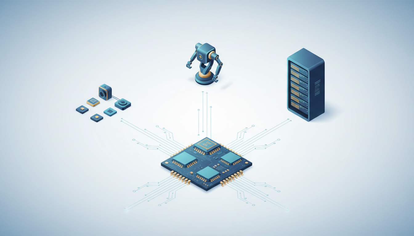
Ceva unveiled a four-tier NeuPro neural processing unit (NPU) portfolio on October 28, 2026, extending its licensable semiconductor architecture from tiny always-on sensors to large-language-model inference in data centers. The Maryland-based company says the common architecture and software environment could let chipmakers reuse their development work across different power and performance classes.
The four designs are NeuPro Nano for low-power sensing, Prime for mainstream vision and transformers, Max for multimodal edge AI and robotics, and Ultra for AI infrastructure. These are processor intellectual-property cores that customers can integrate into custom chips—not four finished processors already shipping to consumers.
Performance claims need independent testing
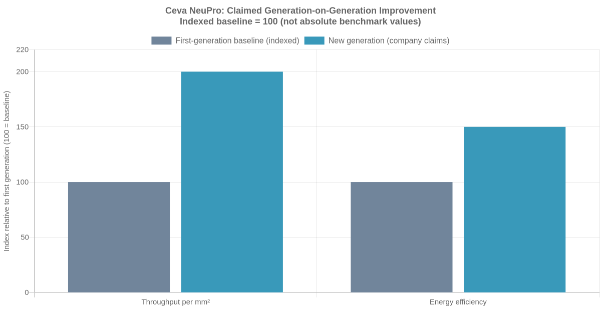
Ceva claims the new architecture offers up to twice the AI throughput per square millimeter and 50% better energy efficiency than the previous generation. Those are vendor-reported improvements, not independently reproduced benchmarks. The accompanying chart uses a normalized old-generation baseline of 100; it does not imply that any specific application doubles its performance.
Technical changes include FP4 and FP8 low-precision arithmetic, improved tensor utilization, dynamic tensor shapes and paged key-value caching for memory-intensive transformer inference. Support for Mixture-of-Experts and linear-attention models is intended to let designers run more varied workloads without replacing the entire NPU architecture.
From sensors to memory-side inference
Ultra moves Ceva into a particularly contested market: integrating inference near memory, connectivity and data-processing components. That could reduce some transfers between processors and memory, although actual system savings will depend on a customer’s silicon, memory bandwidth and workload. The proposal differs from standalone BrainChip AKD1500 developer hardware and from cloud-oriented Xeon inference software.
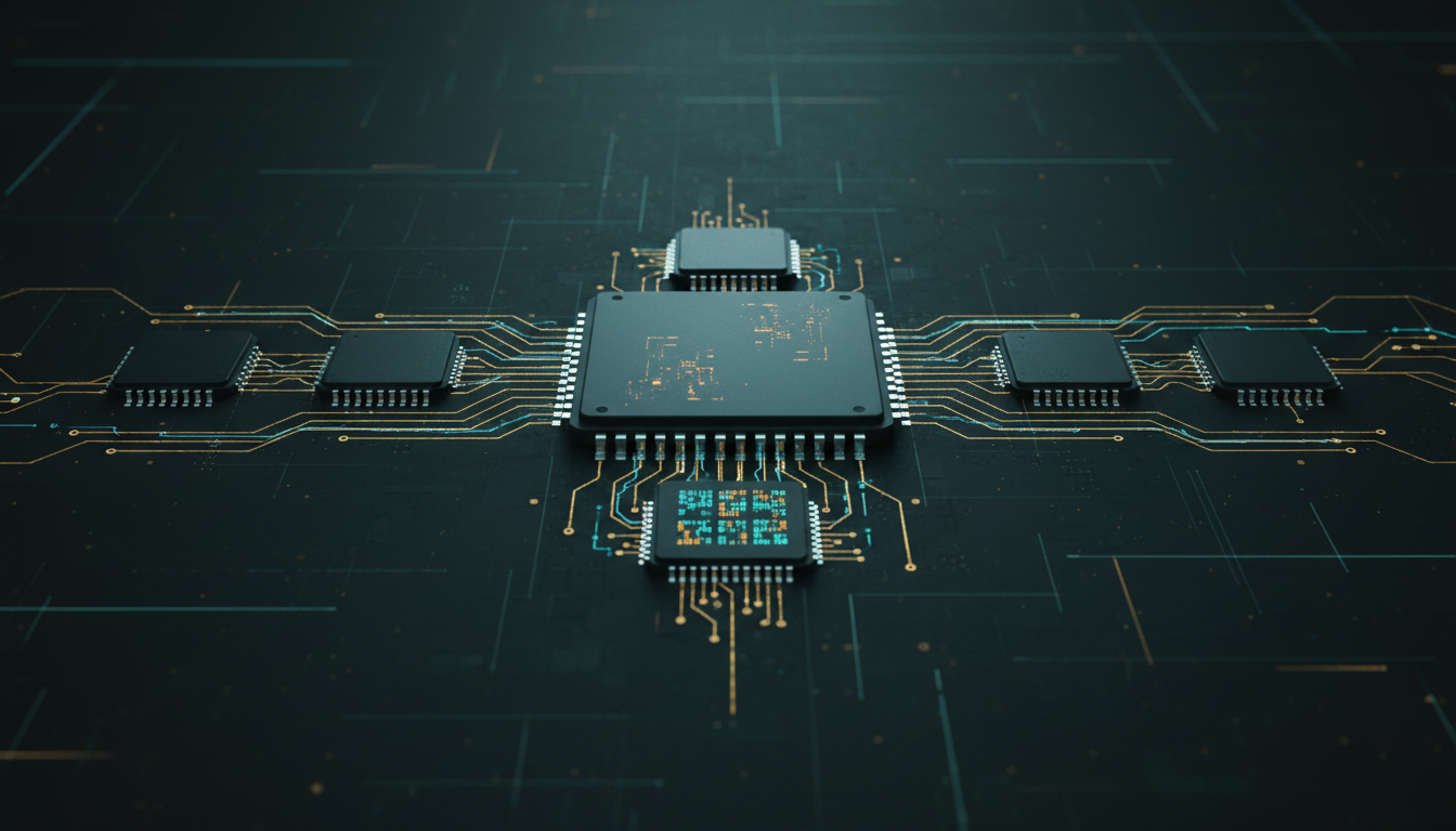
A unified development kit should help customers scale designs from edge products to larger systems. For comparison, Google and Synaptics have pursued embedded AI processors, while Infineon has emphasized physical AI across robotics, vehicles and infrastructure. A shared vocabulary does not mean the products are interchangeable.
Ceva says selected customers are already evaluating the architecture, with general availability planned for the second quarter of 2027. It has not disclosed validated customer-chip shipping volumes, priced implementations or comparable independent energy tests for the new family.
The immediate milestone is customer integration, not a claimed data-center breakthrough. Engineers will need real workload benchmarks, memory traffic measurements, power results and software support before deciding whether NeuPro Ultra makes a meaningful difference to AI infrastructure connectivity or on-device inference.
Editor’s Note: We volunteer daily to ensure the credibility of the information on this platform is Verifiably True. If you would like to support our work and help further secure the integrity of our research initiatives, please scan the QR code below to donate 5,000 sats.

For mobile scanning, open this story on a laptop or larger display and scan the original QR code with a compatible Bitcoin wallet. Verify the receiving address before sending: 3C9o19EH5HSiwEPyCTmEKzxhNCbo2X6TTb.
BitcoinVersus.tech is not a financial advisor. This media platform reports on financial subjects purely for informational purposes.


Leave a Reply