
A tiny crystal long studied for its ability to control light now has a much clearer optical fingerprint. Researchers at South Korea’s KAIST, working with Caltech and other partners, have measured how barium titanate (BaTiO₃, or BTO) bends and absorbs light over wavelengths from 190 nanometers to 40 micrometers. The results, announced by KAIST on November 8, 2026 and published in ACS Photonics on October 20, could help engineers design lower-loss optical components. The work characterizes a material; it does not demonstrate a faster commercial internet connection.
Sourcery’s May 2026 tour shows PsiQuantum growing barium titanate thin films for a separate photonic-chip program. The factory footage is independent background, not a demonstration of the KAIST–Caltech measurement or its performance. Watch the full wafer-manufacturing visit.
Why a light-control crystal needed better data
Barium titanate is ferroelectric, meaning it can maintain electrical polarization. Applied voltage can also change its optical refractive index through the Pockels effect. A photonic modulator can exploit that response to encode electronic data onto a traveling optical signal. However, designers need two different measurements: refractive index, indicating how light propagates, and extinction coefficient, describing absorption. Misjudging either can produce inefficient waveguides, unexpected insertion loss or inaccurate simulation results.
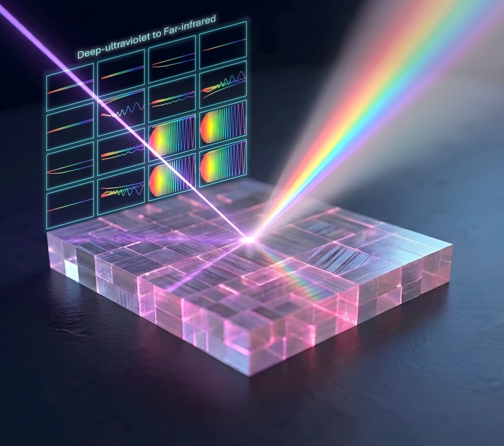
The difficulty has been the crystal’s microscopic domains. Neighboring regions can point in different crystallographic directions, and each orientation interacts differently with polarized light. Older measurements often averaged those responses together, generating conflicting optical constants. The team instead examined two types of relatively uniform single-crystal samples and used Mueller-matrix spectroscopic ellipsometry to separate polarization-dependent behavior.
The measurements span more than a 200-fold wavelength range
The lower end of the test is 190 nm, in the ultraviolet. The upper end is 40 μm, or 40,000 nm, in the far infrared. Dividing 40,000 by 190 gives about 211 times the wavelength, not a 211-fold increase in data speed. The researchers divided the spectrum into three analysis regions and modeled how crystal orientation changes light propagation. Broad measurements matter because material properties cannot safely be assumed constant from one wavelength band to another.
In a particularly transparent part of the material, KAIST reports extinction coefficients around 10⁻⁵ between 2 and 10 μm, confirmed using separate transmission measurements. The commonly used fiber-optic C-band around 1.55 μm falls outside that 2–10 μm interval. Engineers therefore should not transplant the cited infrared loss number directly into a telecom-link budget or treat it as complete device insertion loss.
Cell Press’s June 2026 webinar discusses reconfigurable photonic hardware with phase-change materials. The technologies differ from BTO’s electro-optic behavior; the presentation provides general photonics context, not independent validation of the new measurements. Watch the researchers’ webinar.
Better simulations before expensive fabrication
The researchers also proposed calculating a crystal’s aggregate optical response from the orientations and proportions of its domains. That could reduce repeated trial-and-error runs when engineers model waveguides, wavelength converters or quantum-photonic circuits. More reliable material inputs are valuable, but device performance will still depend on interfaces, film thickness, propagation length, fabrication defects and electrical drive circuits.
Related BitcoinVersus.Tech coverage includes an 8×8 photonic switch, reported optical-switch loss reductions, 800G versus 1.6T pluggable optics, and long-haul hollow-core fiber experiments. Each reports a distinct metric, so crystal absorption, switch insertion loss and end-to-end network throughput should not be compared as interchangeable results.
What remains to be proven
The next meaningful milestone is a manufactured BTO device with independently measured modulation bandwidth, drive voltage, optical insertion loss, thermal stability and manufacturing yield. None of those commercial-performance measures was established by the new bulk-crystal characterization alone. The achievement is a more dependable design reference, rather than proof that existing networks can immediately transmit faster.
Primary documentation: KAIST News Center, November 9; Kang and colleagues, ACS Photonics, October 20, 2026. The 211-fold wavelength ratio is independently calculated from the reported endpoints; no network-speed gain is inferred.
We volunteer daily to ensure the credibility of the information on this platform is Verifiably True. If you would like to support to help further secure the integrity of our research initiative, please scan the QR code below.



Leave a Reply