semiconductors
-

A lattice atom refers to an atom that occupies a regular, repeating position within the crystal lattice of a solid material. In crystalline solids, atoms are arranged in a highly ordered structure known as a lattice, where each atom is situated at a specific point defined by the geometry of the unit cell. These lattice…
-
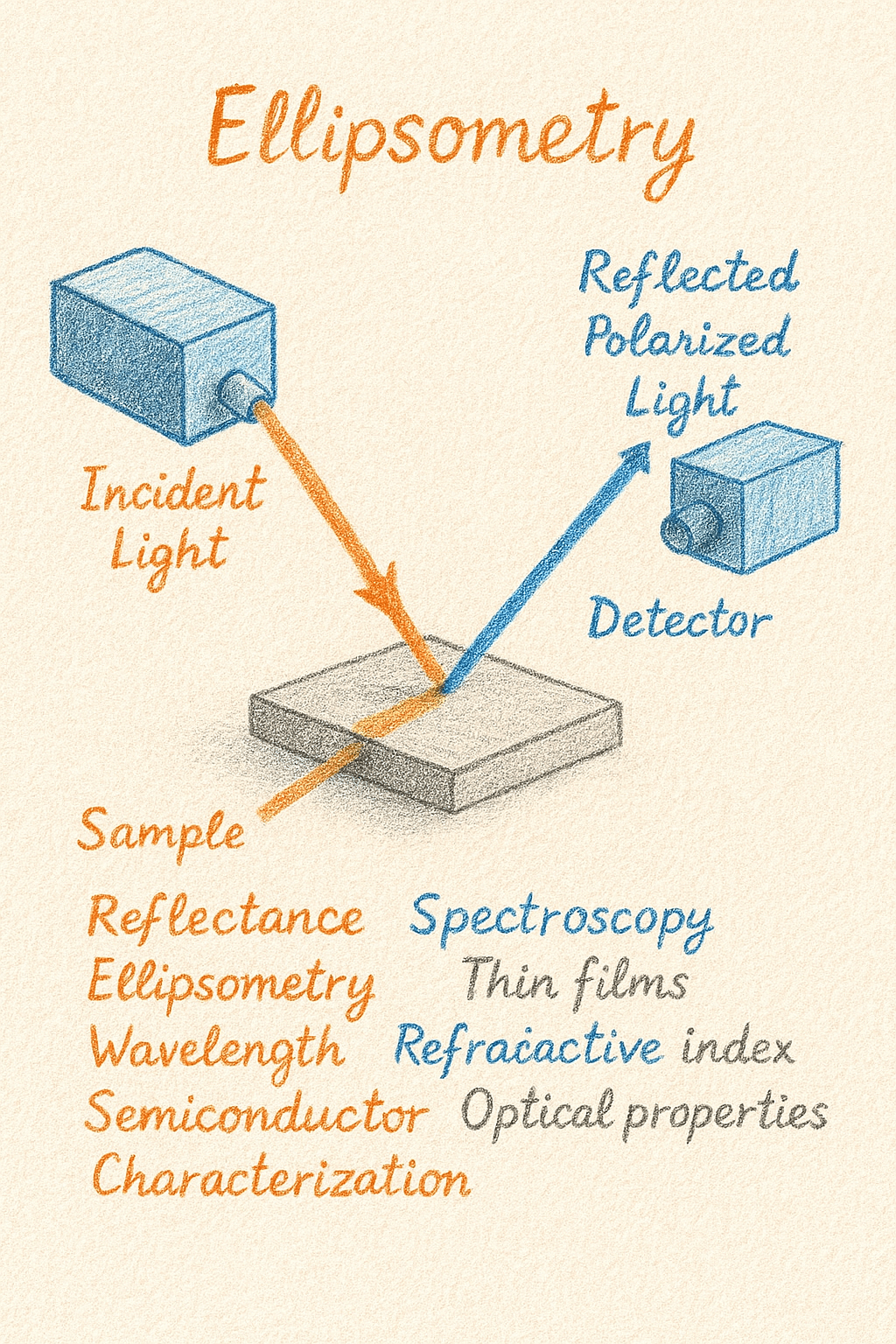
Ellipsometry is an advanced optical technique used to characterize thin films and surfaces by analyzing changes in the polarization of light upon reflection or transmission. In practice, a beam of polarized light is directed at a material, and the reflected or transmitted light undergoes a change in polarization that is measured as two parameters: the…
-
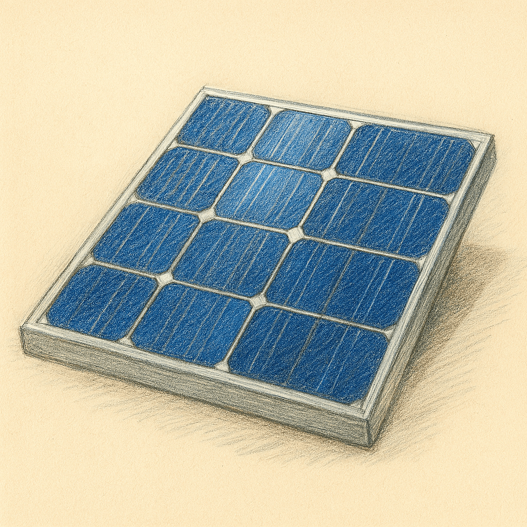
Solar cell roughness characterization is the process of analyzing and quantifying the surface texture of photovoltaic materials to understand how microscopic topographical features influence optical and electrical performance. The surface of a solar cell—whether crystalline silicon, thin-film, or emerging materials like perovskites—plays a critical role in determining how light interacts with the device. Controlled roughness…
-

Auger Electron Spectroscopy (AES) is a powerful surface-sensitive analytical technique widely used in materials science to investigate the elemental composition of the outermost atomic layers of a sample. Unlike bulk characterization methods, AES focuses specifically on the top few nanometers of a material, making it invaluable for studying thin films, coatings, and surface modifications. The…
-

Polycrystalline silicon, often called poly-si, is a special material used to build the tiny pathways inside computer chips. Its main job is to control the flow of electricity, and a key property it has is called resistance. Resistance is how much a material slows down or fights against the electric current. Think of it like trying…
-

The solar energy industry traces its roots to nineteenth century scientific discoveries, beginning with the photovoltaic effect identified by Edmond Becquerel in 1839 and early selenium based cells in the late 1800s. It did not become a modern commercial sector until Bell Labs created the first practical silicon solar cell in 1954, which initially found…
-

Electron beam characterization involves using a focused beam of electrons to probe and analyze materials at very fine scales. Techniques such as scanning electron microscopy (SEM) and transmission electron microscopy (TEM) rely on the interaction between electrons and the atoms in a sample to reveal details about surface morphology, internal structure, and even chemical composition.…
-
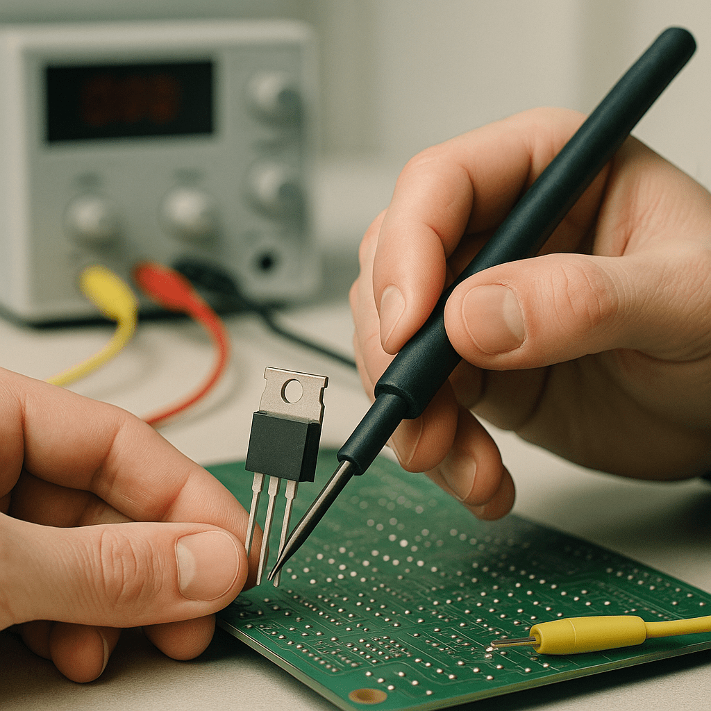
The source‑series resistance (Rₛ) and drain‑series resistance (Rᴅ) are the parasitic resistances that appear in series with the source and drain terminals of a MOSFET. They arise from the silicon substrate, metallization layers, and package leads that connect the internal transistor to the external pins. When the device is turned on, the total on‑resistance (Rₒₙ)…
-
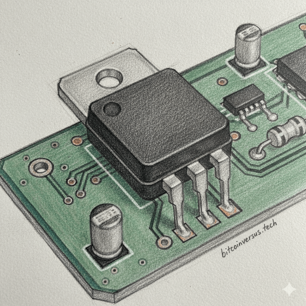
MOSFETs, or Metal-Oxide-Semiconductor Field-Effect Transistors, are essential components in modern electronics, and understanding their operating characteristics is crucial for anyone interested in electronics. These devices function as switches or amplifiers, controlling the flow of electrical current. The key to their operation lies in the voltage applied to the gate terminal, which influences the conductivity between…
-

Understanding oxide charge density in semiconductors is an important concept in electronics and materials science. Semiconductors are materials that have electrical properties between those of conductors and insulators. They are essential for making electronic devices like computers and smartphones. The oxide charge density refers to the amount of electric charge that is stored in the…
-

The flatband capacitance (CFB) is defined as the total measured capacitance of a Metal-Oxide-Semiconductor (MOS) structure or a similar semiconductor device when the applied gate voltage is exactly equal to the flatband voltage VFB. This flatband voltage represents the specific potential needed to establish the flatband condition, where the energy bands within the semiconductor substrate…
-

Metal oxide semiconductor capacitance voltage measurement is a way to electrically study what is happening at the surface of a semiconductor under a gate. The structure used is a simple capacitor made of a metal gate on top, a very thin insulating oxide in the middle, and a semiconductor such as silicon on the bottom.…

