semiconductors
-

Singapore’s ST–NUS HELIX Corporate Lab is targeting edge and embodied AI with 18nm FD-SOI, embedded phase-change memory, in-memory computing and memory-centric architectures.
-
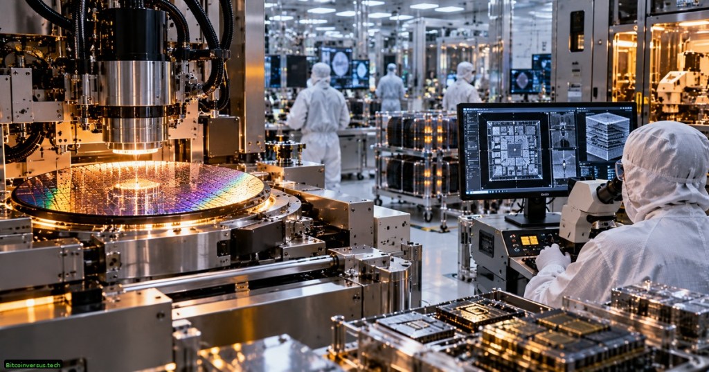
Applied Materials and Intel are linking Silicon Valley and Oregon R&D to accelerate next-generation transistors, interconnect scaling and Foveros-based 3D packaging for AI chips.
-

TSMC is evaluating a possible Texas investment just as one of its biggest advanced-chip customers is asking for more capacity. The timing matters because AMD CEO Lisa Su said on October 6 that the company plans to substantially increase chip supply in 2027 and needs more advanced wafer capacity over the next several years. TSMC…
-
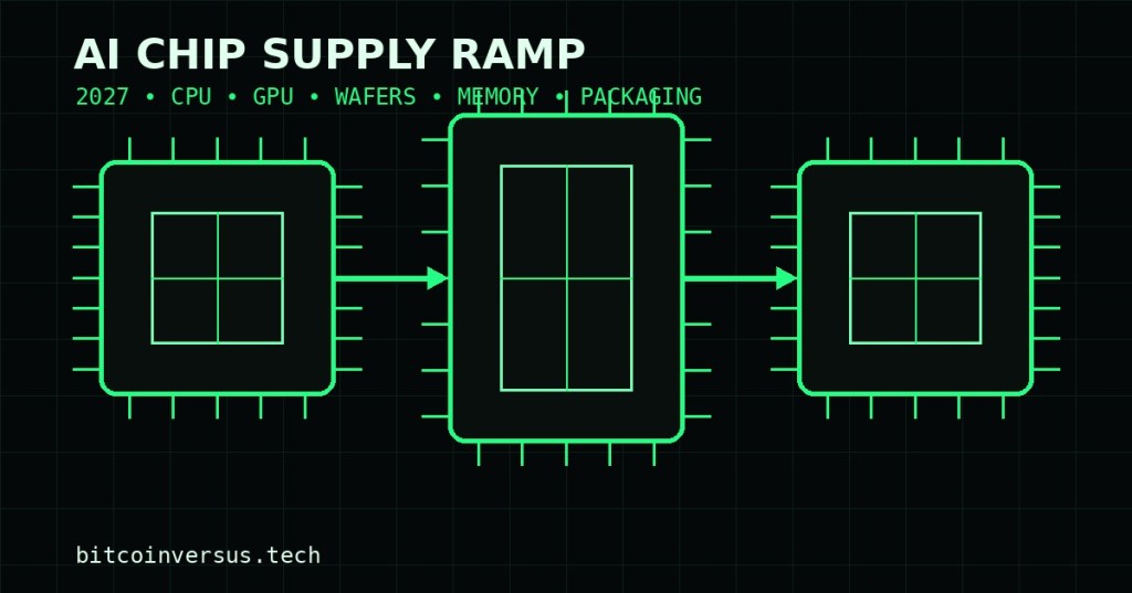
AMD plans to substantially increase CPU and GPU supply in 2027 as AI demand strains advanced wafers, HBM, packaging and rack-scale manufacturing capacity.
-
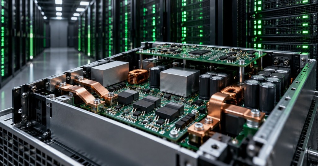
Microchip and Navitas have built a 20 kW 800V-to-6V AI rack reference design targeting 96% efficiency, 1 MHz switching and 2,100 W/in³ power density.
-
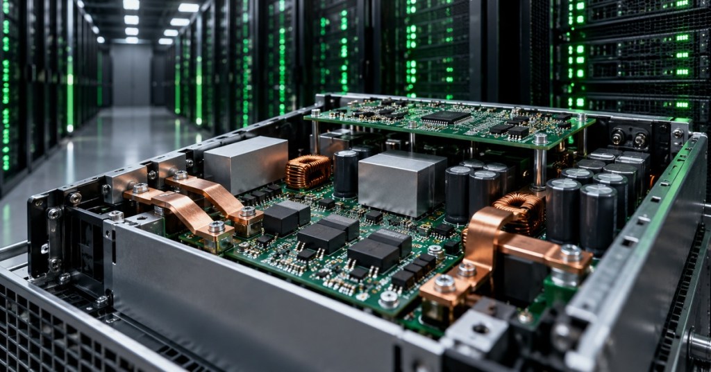
Microchip and Navitas unveiled an 800V DC-to-6V GaN reference design for AI racks, combining digital control, hardware security and OCP-aligned power.
-

AMD Ross connects agentic AI to Vivado, Vitis HLS and embedded engineering workflows through MCP servers, reusable skills and AMD technical knowledge.
-
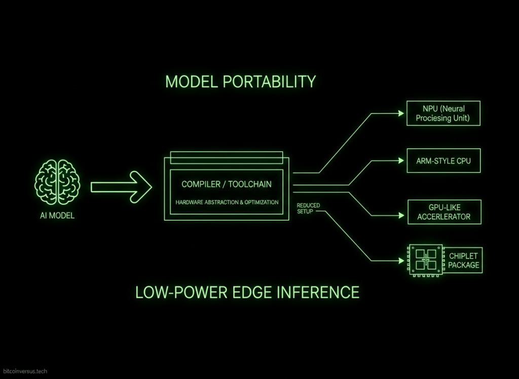
Lola Vision Systems is attacking the roughly 200-hour setup burden of moving AI models onto new edge chips with an automated compiler toolchain while developing its own five-chiplet processor.
-
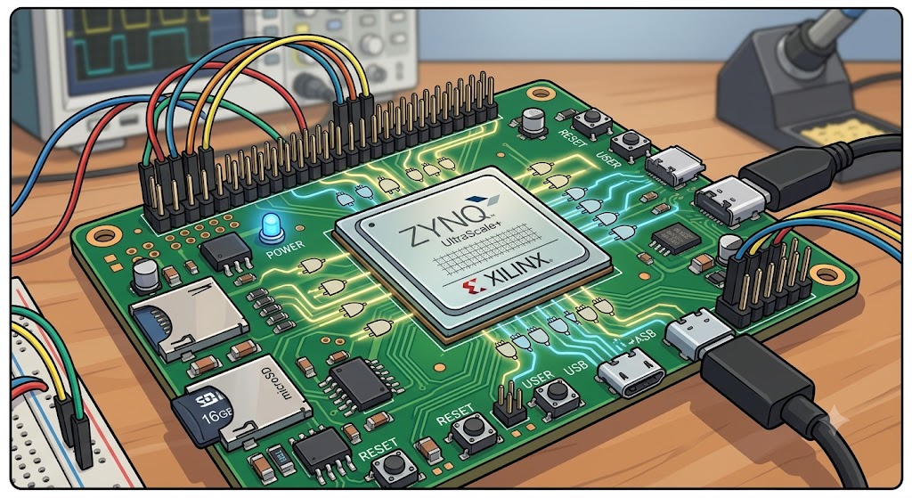
A Field-Programmable Gate Array, or FPGA, is a semiconductor device that can be configured after manufacturing to perform custom digital logic functions. Unlike a traditional CPU, which executes software instructions sequentially, an FPGA contains programmable logic blocks, routing resources, memory elements, and digital signal-processing components that can be arranged into specialized hardware circuits. Engineers commonly…
-
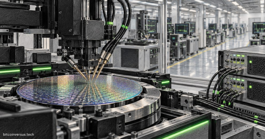
ASE Singapore approved a 449,340-square-foot Yishun factory purchase on September 29, creating room for future chip capacity expansion while operational details remain unconfirmed.
-
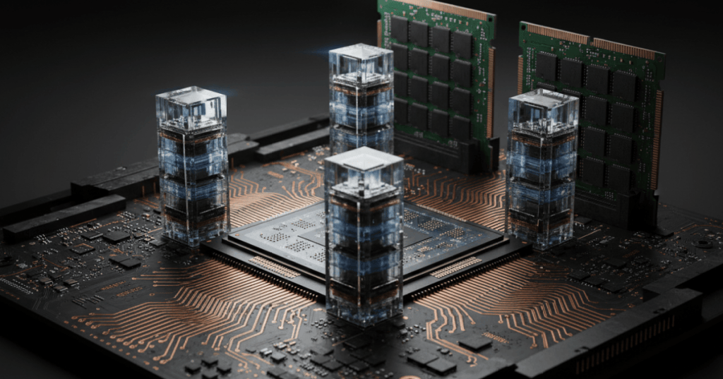
AI demand for HBM is consuming a growing share of DRAM wafer capacity, tightening conventional memory supply and helping push ordinary RAM prices higher.
-
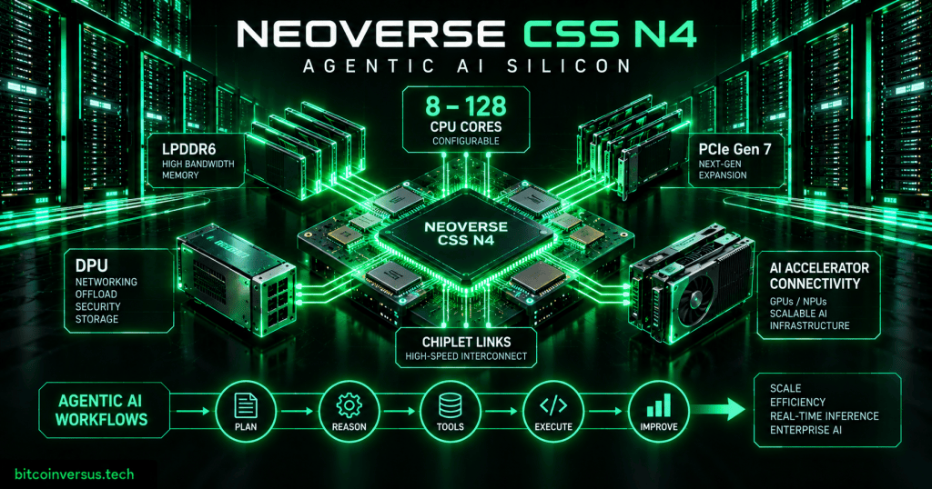
Arm’s Neoverse CSS N4 gives chip designers a configurable 3nm-class foundation with up to 128 CPU cores, LPDDR6, PCIe Gen 7 and high-speed AI accelerator connectivity.

