semiconductors
-
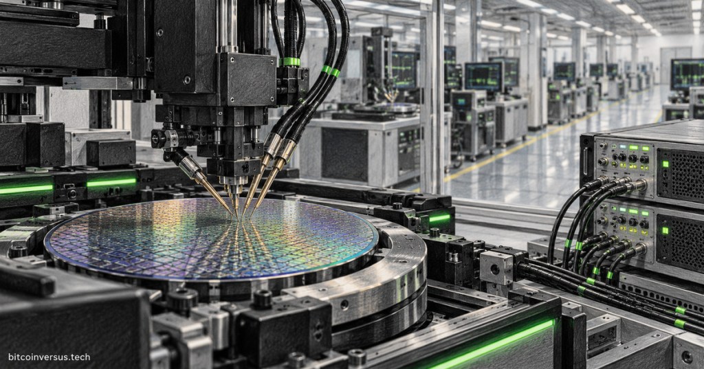
ASE Singapore approved a 449,340-square-foot Yishun factory purchase on September 29, creating room for future chip capacity expansion while operational details remain unconfirmed.
-
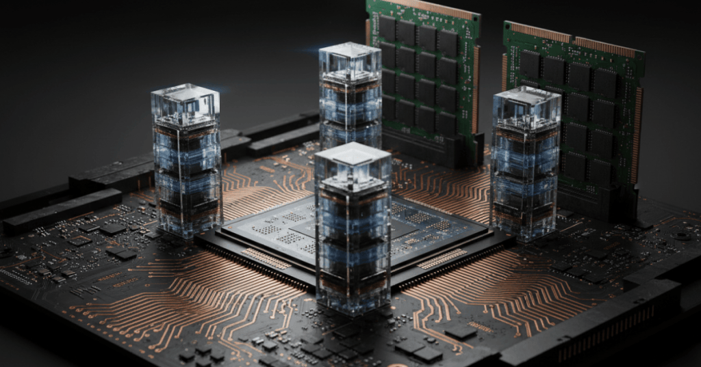
AI demand for HBM is consuming a growing share of DRAM wafer capacity, tightening conventional memory supply and helping push ordinary RAM prices higher.
-
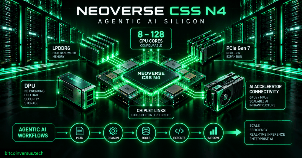
Arm’s Neoverse CSS N4 gives chip designers a configurable 3nm-class foundation with up to 128 CPU cores, LPDDR6, PCIe Gen 7 and high-speed AI accelerator connectivity.
-
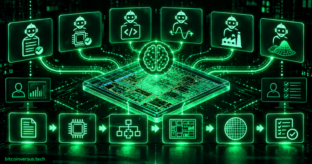
Synopsys’ new Autopilot Platform coordinates long-horizon AgentEngineer systems across verification, implementation, analog design, manufacturing and simulation workflows.
-

OpenAI says AI-assisted engineering helped move its Jalapeño inference chip from RTL execution to tapeout in roughly nine months, offering a glimpse at how AI could reshape semiconductor design.
-
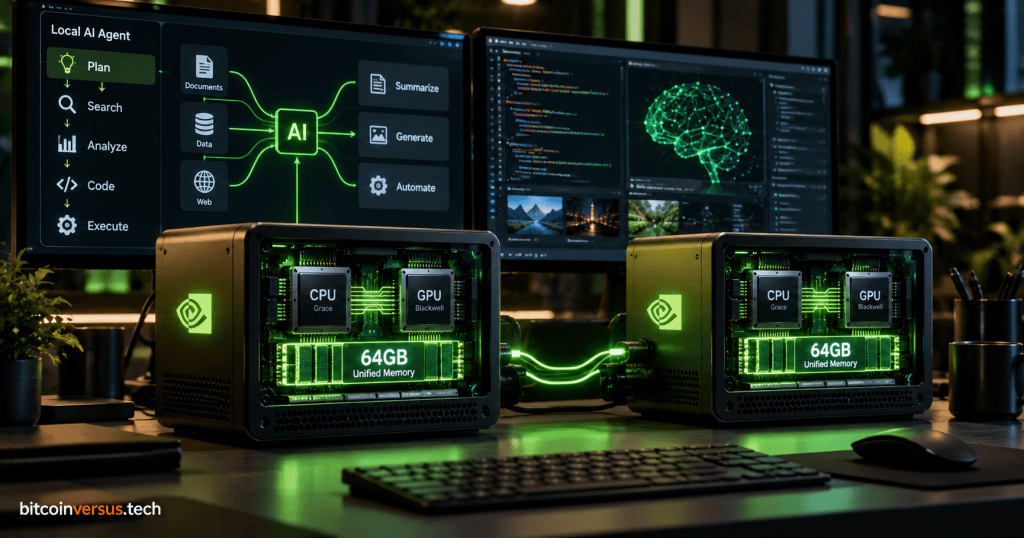
NVIDIA is adding a 64GB DGX Spark configuration that keeps the GB10 Grace Blackwell platform and adds two-system clustering for larger local AI-agent workloads.
-
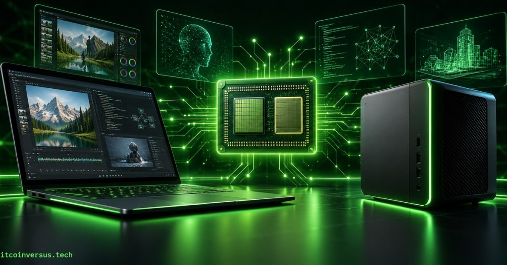
NVIDIA RTX Spark Windows PCs arrive in October with Grace and Blackwell silicon, up to 128GB unified memory, local AI agents and NVIDIA PAIR.
-
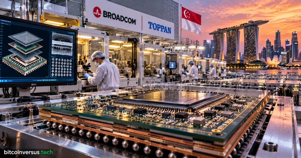
Broadcom and TOPPAN joint venture Advanced Substrate Technologies has opened Singapore’s first high-end FC-BGA substrate factory, targeting a critical AI-chip packaging bottleneck.
-
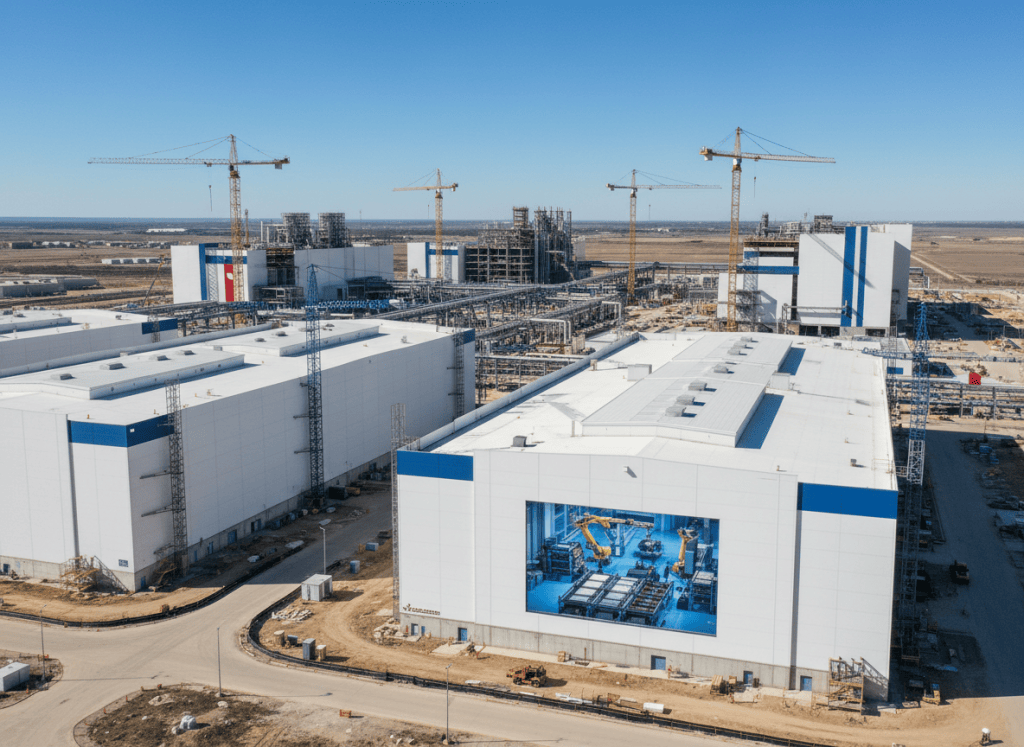
Elon Musk confirmed that Terafab is in discussions with TSMC, but no semiconductor manufacturing partnership has been announced.
-
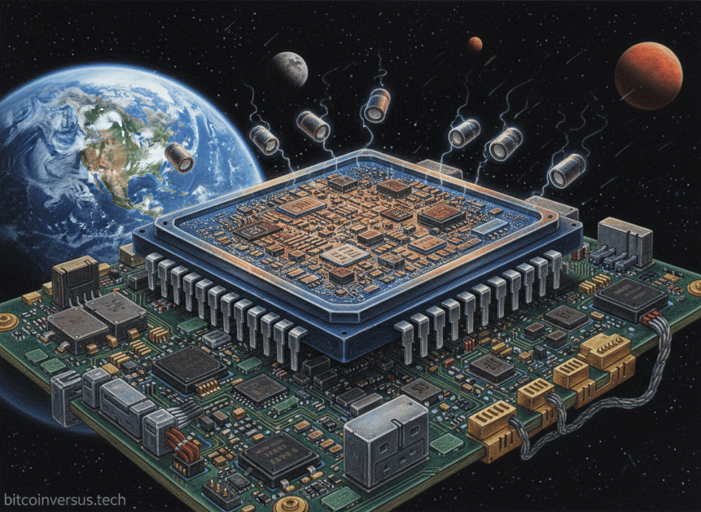
AMD is sampling the XQRVC1902 Versal AI Core adaptive SoC in an enhanced space-grade package designed for missions lasting up to 15 years and headed toward Class Y qualification.
-
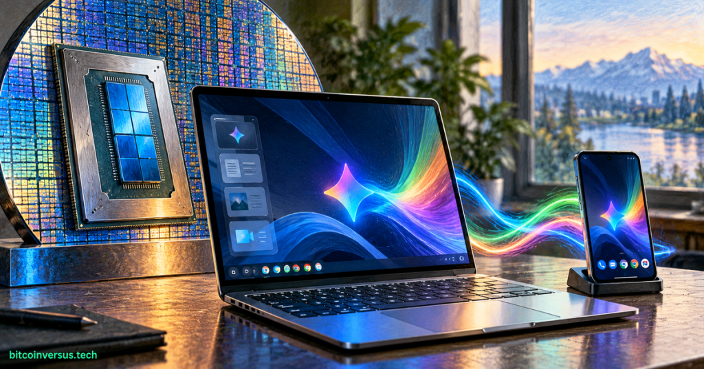
Googlebook gives Intel Core Ultra Series 3 a high-profile new showcase: three of the five launch systems use Panther Lake, putting Intel 18A into direct competition with Snapdragon X Elite inside Google’s new premium laptop platform.
-
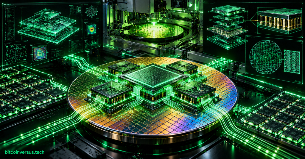
Cadence and TSMC are combining A14-certified design flows, UALink, UCIe-64G and 3DFabric support for wafer-scale AI systems containing hundreds of chiplets.

