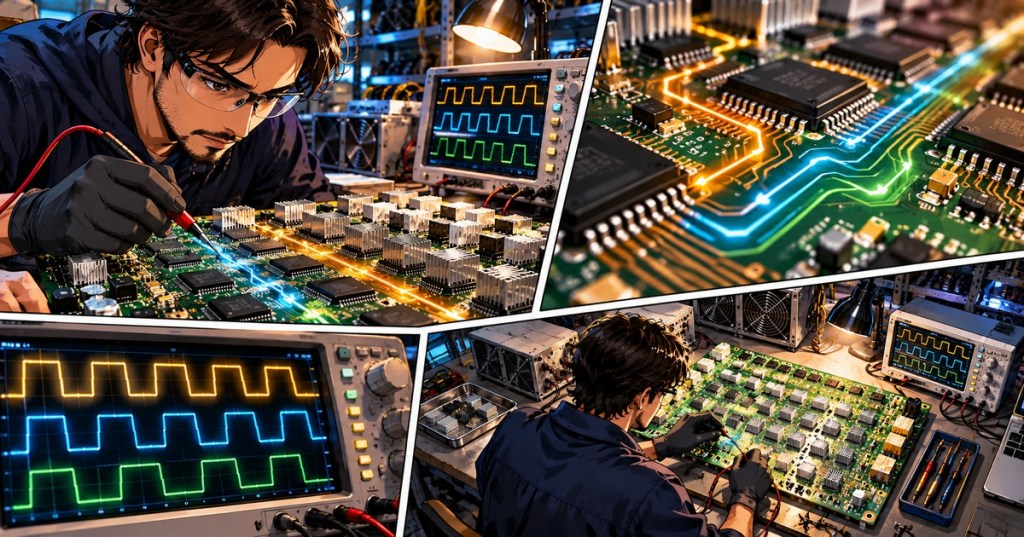
OSHRE.002 — Open-Source Hashboard Repair Engineering / Super-Fundamentals. A Bitcoin mining ASIC cannot work in isolation from its neighbors: it must receive timing and commands, recognize reset and status conditions, and return calculated results. On the classic Antminer S9, five labeled signal families organize that communication: CLK, CO, RI, BO and RST. A repair engineer must understand both the meaning of each signal and the direction it travels before interpreting missing-chip symptoms. This lesson builds on OSHRE.000, The Anatomy of the Hashboard, and OSHRE.001, Hashboard Voltage Domains and Power Distribution.
Learning objectives
- Identify the purpose of CLK, command in/out, result return, busy/status and reset in an ASIC chain.
- Trace the forward and reverse paths in a documented 63-chip BM1387 Antminer S9 board.
- Explain why a 25 MHz oscillator and chip-internal hashing clocks are not interchangeable performance specifications.
- Interpret incomplete chip enumeration as diagnostic evidence, not automatic proof that all missing ASICs are defective.
- Build a de-energized intake worksheet and distinguish safe observation from energized electrical diagnosis.
1. What is an ASIC signal chain?
A signal chain is the organized succession of electrical communication links among mining chips and the board’s controller-facing circuitry. It is related to—but separate from—the electrical voltage domains that supply energy to those chips. The command stream travels toward the later ASICs in the chain, while responses can travel in the opposite direction. Reset, clock and status paths supply additional coordination. The precise interface is a property of the chip family and PCB revision, not a universal protocol shared by all Bitcoin miners.
In the reference S9, ZEUS MINING’s S9/S9i board documentation identifies 63 BM1387 chips, numbered from 00 to 62 in one service-guide convention (or U1 through U63 on other diagrams). It distinguishes four signals that propagate forward and one response path that returns in reverse. That directional distinction is the heart of this lesson.
2. The five signal families at a glance
| Label | Common interpretation | Documented S9 direction | Why it matters |
|---|---|---|---|
| CLK | Clock / timing reference | Oscillator through early ASICs toward chip 62 | A missing or malformed clock can prevent valid synchronous chip operations. |
| CI / CO (TX) | Command input / output | Controller side → chip 00 → chip 62 | Moves work/control information forward along the chip chain. |
| RI / RO (RX) | Response input / output | Chip 62 → chip 00 → controller side | Returns computed results and responses toward the host. |
| BI / BO | Busy/status path | Chip 00 → chip 62 in S9 service description | Supports chip status/flow signaling; purpose and levels vary by implementation. |
| RST / NRST | Reset signaling | Controller side → chip 00 → chip 62 | Places the chain in a defined reset/startup state when properly asserted. |
In chip documentation, the suffix I generally denotes an input and O an output. Thus a chip can accept a command at CI and forward it through CO, or receive a return response from the next device at RI and pass it back through RO. The familiar uppercase labels are convenient, but pin-number assignments, active-low conventions, pad locations and electrical interfaces must always be checked against the actual silicon package and board revision.
3. The physical ASIC package and the surrounding board
Signals travel through copper traces, solder joints, capacitors, resistors and, at some voltage boundaries, translation or coupling circuitry. They do not jump wirelessly from one package to the next. The original photograph below shows a real BM1387B package and its PCB environment. The photography documents physical hardware; it is not a synthetic drawing of chip pins or an authorized live-probing map.
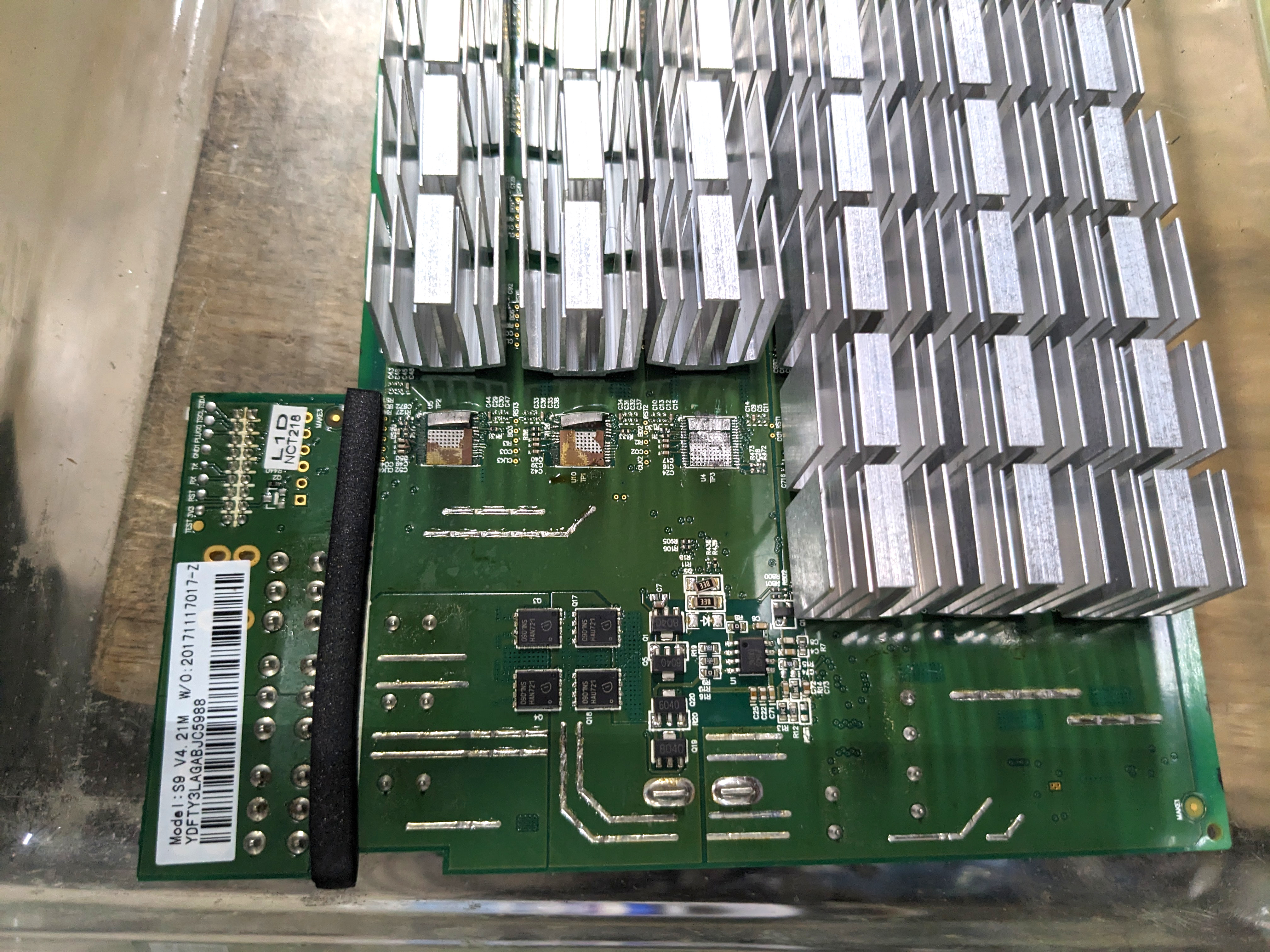
A chip can have intact power but fail to communicate because an upstream signal is missing. Conversely, a healthy signal path does not prove that every chip has adequate core supply or thermal contact. In repair records, keep power-domain observations, signal-chain observations and measured hashing performance distinct; this prevents a symptom in one subsystem from being prematurely assigned to another.
4. Clock signal — CLK
According to the S9 hashboard repair guide, the reference design uses a 25 MHz oscillator at Y1. The external clock path propagates through the ASIC chain; inter-device connections can include capacitive coupling. A clock is a timing reference, not a direct count of completed SHA-256 hashes. Chip-internal circuits can use other clocking and timing structures, so 25 MHz must not be multiplied by chip count to infer the miner’s TH/s.
An oscilloscope waveform viewed in a training video should be interpreted in terms of its own measurement reference, frequency, amplitude, duty cycle and probe loading. A handheld DC meter does not display the full switching waveform; an averaged reading is not equivalent to a validated clock signal. To review clock concepts outside mining, see What Is a Clock Signal?
5. Command and return paths — CO and RI
For the reference S9, command traffic is passed forward from the host connection toward successive ASICs. Return traffic follows the opposite direction toward the host. The repair guide identifies this as TX/CI–CO versus RX/RI–RO. That does not make the chip chain an Ethernet cable, and these labels are not interchangeable with general network-layer transmit/receive ports. The control board and firmware manage work distribution, while ASIC-level signaling takes place across the board’s specialized electrical interface.
When one link is open, shorted, improperly powered or unable to relay data, the controller can lose communication with additional devices that are physically present and potentially healthy. This is why an observed “ASIC count” is an enumeration result rather than a headcount of chips that must be replaced. It is essential to record the indexing convention—0-based or 1-based—before mapping a reported number to a physical package.
6. Reset and busy/status paths — RST and BO
RST is the reset-related path. On a device using active-low reset conventions, assertion and release correspond to defined logic states; the exact levels and timing depend on the chip and test state. BO, commonly described as the B or busy-pulse signal in S9 service literature, is another forward-propagating chain signal. A low DC value at a designated point is not independently proof of failure: it can reflect standby operation, a pulsed signal averaged by the instrument, or a model-specific state.
ZEUS MINING’s test-point explanation explicitly lists the S9’s four forward paths as CLK, CO, BO and RST, with RI returning in reverse. Older repair guides publish illustrative operating voltages, but those values should never be treated as universal instructions for newer devices, different control fixtures or unknown PCB revisions.
7. Video study — locating the fault range using an S9 test fixture
The following original ZEUS MINING recording focuses on the relationship between test-fixture observations and the region of a suspected ASIC fault. While watching, note when a displayed chip count narrows the search versus when the technician needs additional evidence. A test fixture detects a communication symptom; it does not automatically reveal the root cause.
For example, consider an illustrative board with 63 expected chips and a fixture that enumerates 42. There are 21 chips not confirmed by that scan, but the figure alone does not prove that 21 chips have failed. Possible explanations include a damaged interface near the transition, a broken return line, inadequate domain power, incorrect fixture or firmware compatibility, or multiple simultaneous defects. The first diagnostic task is to validate the model and fixture, then compare observations with the correct documented signal directions.
8. Tracing a symptom without assuming a diagnosis
| Observed condition | Plausible systems to investigate | What the observation does not establish |
|---|---|---|
| Controller sees zero chips | Power delivery, ribbon connector, fixture, reset, clock, controller interface, chain links | That every ASIC package is destroyed. |
| Partial chip count | Signal relay near the reported boundary, return path, domain power, clock, solder connection | That the first unreported chip is definitely faulty. |
| Fluctuating count | Temperature, unstable supply, connector integrity, clock quality, intermittent joint | That a reflow operation is necessarily the correct repair. |
| All chips enumerate but hashrate is low | Work configuration, core supply, thermal limits, share/error behavior, clocks | That chain continuity alone guarantees hashing performance. |
The S9 missing-ASIC case guide describes using the reported chip number to choose the neighborhood for further testing, while also distinguishing “ASIC=0” cases that could involve cables or controller hardware. This is a process of narrowing hypotheses through evidence—not proof that a single error message uniquely identifies one defective solder joint.
9. Video study — full S9 board diagnosis
ZEUS MINING’s second original repair video demonstrates broader S9 board-level fault diagnosis. Focus on how the technician relates the physical board, test equipment and diagnostic outcome. The procedure shown is professional electronics service and must not be reproduced on an energized unit by an untrained learner.
When reviewing both recordings, answer: Which measurements concern chip power and which concern communication? Does a test identify the first missing response, or does it demonstrate the exact failed component? Does the video document the same board revision as the one you are studying? Separating these questions prevents the most common category error in chain troubleshooting.
10. Model differences and board revisions
Not every chip chain has 63 devices, the same connector, or the same physical test-point order. In ZEUS MINING’s Antminer S17 guide, the documented BM1397AD board carries 48 ASICs in 12 voltage domains, and the same broad signal labels are used. Another product may change chip population, timing design, level-shifting approach or board layout. For why identical-looking modules should not be assumed compatible, review hashboard interchange limitations.
The S9’s five familiar signals are a useful educational vocabulary, not a license to use an S9 fixture, cable or test-point reference on an S17, S19, S21, WhatsMiner or Avalon design. Always begin with the exact PCB silkscreen, revision, chip part number and supported manufacturer service procedure.
11. Safety boundary and unpowered training exercise
Electrical warning: An ASIC miner combines mains-derived power, high-current DC conductors, stored energy, hot heatsinks and domain-dependent measurement references. Bridging two test points with a probe or contacting a conductive heatsink can cause equipment damage or injury. This introductory lesson contains no authorization for energized probing, power injection, chip rework or oscilloscope ground connection. Such operations require training, authorization, isolation plans, correctly rated instruments and model-specific procedures.
For a classroom assignment, use the real photographs in this article or a board that a qualified person has isolated, discharged and verified safe. Record only visible markings and the documented signal names. Then complete a paper-only logic exercise:
- Write the documented S9 forward path as controller → chip 00 → chip 62 for CLK, CO, BO and RST.
- Write the response path in the reverse direction as chip 62 → chip 00 → controller for RI/RO.
- Explain why a reported count of 42 of 63 chips leaves 21 unconfirmed devices but does not identify the actual failed component.
- Make a list of observations that require model-specific evidence: PCB revision, cable pinout, test-point positions, logic voltage and expected reset behavior.
- Summarize which details you can determine from physical inspection alone and which require protected test procedures or verified measurements.
12. Knowledge check and answer key
- Which of the five classic S9 signal families returns from the end of the chain toward the control board?
- What is the external oscillator frequency identified in the S9 repair documentation?
- Why is that oscillator frequency not equal to the Bitcoin miner’s total hashing rate?
- If a 63-chip board enumerates only 42 devices, how many are unconfirmed by the test? Does that prove all 21 are defective?
- Name two plausible causes of incomplete ASIC detection other than a failed mining chip.
- What must be verified before applying any test-point reference from a repair video?
Answers: (1) RI/RO, the response path. (2) 25 MHz for the documented S9 reference. (3) The oscillator synchronizes circuitry; hashing throughput depends on internal chip architecture and operating conditions, not simple multiplication of the external clock. (4) 21 are not confirmed, and no, their failure is not proven. (5) Examples include a cable fault, missing clock, unstable domain power, reset problem or faulty controller interface. (6) Exact model, PCB revision, schematic, proper reference, isolation and trained safe-test conditions.
13. References and continued study
Primary technical references are the S9 hashboard repair guide, five-signal test-point documentation, S9/S9i model overview and BITMAIN’s low-hashrate support material. These sources describe a specific generation and should not be transplanted to an unverified board. The next OSHRE foundation lesson can focus separately on unpowered PCB identifiers and test-point literacy, rather than jumping directly into energized fault repair.
BitcoinVersus.Tech — Independent open technical education.
BitcoinVersus.Tech Editor’s Note: This lesson teaches conceptual hashboard signal flow and evidence-based fault classification, not energized repair. If it supports your learning, consider a contribution of 5,000 sats. Scan the original donation QR code below with a compatible Bitcoin wallet, or verify the Bitcoin receiving address 3C9o19EH5HSiwEPyCTmEKzxhNCbo2X6TTb before sending.

Open the QR image on another screen and scan it with a Bitcoin wallet. BitcoinVersus.tech is not a financial advisor. This media platform reports on financial subjects purely for informational purposes.


Leave a Reply