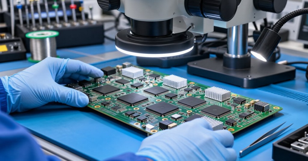
OSHRE.006 teaches the visual inspection of solder connections and printed wiring features on Bitcoin mining hashboards. A hashboard is a densely populated electronic assembly that distributes power, timing and digital signals to specialized ASICs. A poor solder connection, lifted copper pad, damaged passive component or board fracture can interfere with a functioning ASIC chain, yet a low hashrate or an ASIC-count error does not by itself prove that a particular solder joint failed.
The chapter follows OSHRE.005 on cables, connectors, and contact faults, extending the inspection from detachable interfaces into the soldered assembly. Readers should first understand OSHRE.000’s board anatomy, OSHRE.001’s voltage domains and OSHRE.002’s signal paths. No live rework, power probing or unauthorized hardware alteration is required for the lesson.
Learning Objectives and Prerequisites
- Identify the function of solder joints, component terminations, pads, vias and plated-through holes on a high-density printed wiring assembly.
- Distinguish direct visual observations from a confirmed root cause of a miner fault.
- Explain wetting, nonwetting, solder bridging, insufficient solder, mechanical cracking and heat-related discoloration.
- Recognize why shiny versus dull appearance alone is insufficient to accept or reject many lead-free solder joints.
- Understand the differences between openly visible joints and concealed terminations beneath a chip or heatsink.
- Use manufacturer model identification and approved inspection criteria to decide when specialist rework, replacement or escalation is warranted.
- Calculate an illustrative I²R heating estimate and list the assumptions that prevent using the result as an actual board temperature.
Prerequisites: basic electronics, continuity, current, resistance, power, electrostatic discharge (ESD), and the meaning of a de-energized electronic assembly. Useful equipment for a supervised training area includes a stereo microscope or magnifier, diffuse bench lighting, an ESD-controlled workstation, a camera, board documentation and labeled reference photographs. A heat gun or soldering station is not necessary for the inspection-only lab.
A Hashboard’s Construction Changes the Repair Decision
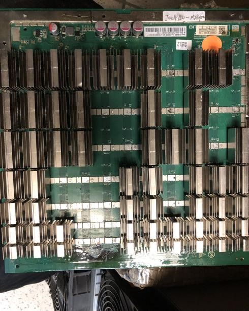
Before inspecting a soldered interface, record the exact manufacturer, miner model, hashboard revision, substrate construction and any service restrictions. Two boards that are casually called “S19 hashboards” may have very different heatsink arrangements and inaccessible joint regions. Bitmain’s S19k Pro support bulletin explicitly differentiates an aluminum-substrate assembly with five large heat sinks from a non-aluminum assembly having 154 chip-related heat sinks across 77 chips. The bulletin also gives different repair-return instructions for the two constructions. These figures apply to the identified S19k Pro variants, not all S19-family hardware.
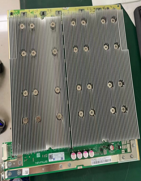
A screw-fastened aluminum heat sink provides a different inspection boundary from soldered-on small heat sinks. Removing thermal hardware without the exact maintenance procedure can create mechanical or thermal damage and alter contact pressure or thermal compound. Do not infer that a visible surface crack always maps to the ASIC beneath it. Obtain the actual board revision and approved service method before proposing a repair.
What Makes an Acceptable Solder Connection?
Soldering creates a metallurgical electrical connection between a component termination and a copper land or conductor. Proper wetting requires suitable surfaces, flux, alloy and thermal process, followed by cooling without damaging movement. A mechanically strong-looking bead is not sufficient proof of electrical continuity, while visible continuity is not proof of reliable thermal cycling or current-carrying performance. Adafruit’s freely available soldering guide and iFixit’s open repair lesson offer accessible examples of wetting, pad heating and common defects.
The industry document IPC-A-610 covers acceptability of electronic assemblies, while J-STD-001 addresses requirements for soldered electrical and electronic assemblies. Their exact criteria depend on the purchased edition, specified class, package type and the product’s controlled documentation. IPC’s public course syllabus identifies solder process, surface-mount, through-hole, cleanliness and component-damage topics, but the syllabus itself is not a substitute for complete acceptance tables. NASA’s Workmanship Standards education site provides a valuable higher-reliability reference and emphasizes trained inspection, ESD controls and documented requirements; NASA flight-hardware rules must not be mislabeled as automatically binding for commercial mining equipment.
iFixit, “Soldering 101: Beginners Guide,” March 28, 2024. Official open-repair education video covering tools, eye protection, fume extraction, through-hole technique and desoldering. It teaches foundational workmanship, not an authorized hashboard repair procedure.
Visible Defects, Likely Mechanisms and Evidence Limits
- Nonwetting or dewetting: solder does not establish the intended bond to a land or termination. Contamination, oxidation or a poorly controlled process may contribute. Photograph the joint before any proposed rework.
- Insufficient solder: incomplete or underfilled fillet where the applicable standard requires a defined connection. Shape, termination geometry and joint accessibility matter more than a universal shine test.
- Solder bridge: unintended conductive solder between adjacent terminals or lands. Treat as a potentially hazardous fault, but confirm the geometry against an approved board revision because some conductors are intentionally connected.
- Cracked joint: an apparent fracture around a solder fillet or component lead, possibly associated with board flexure, vibration or thermal cycling. A line in a photograph may also be flux residue or a harmless surface mark.
- Lifted pad or torn copper: a land or conductor partly separated from the laminate. Heating again may worsen the damage; restoration needs an approved method and qualified specialist.
- Burning or discoloration: localized darkening, melting, or damaged insulation may indicate an overtemperature event. Discoloration alone is not a calibrated thermometer or definitive cause determination.
- Concealed joint: ball-grid-array connections, joints under heatsinks and hidden thermal pads cannot be judged by an exterior photograph. Specialist methods may include X-ray or other nondestructive evaluation when justified.
The iFixit soldering reference notes that lead-free solder joints need not be shiny. A dull surface does not automatically establish a cold joint. Reflective lighting, residue, alloy chemistry and surface texture can affect apparent appearance. Engineers should use the correct magnification and actual acceptance criteria, then correlate visual findings with a repeatable failure and valid test conditions.
Microscopy and Traceable Inspection
Begin with a documented asset identity and approved electrical isolation. Preserve device logs, maintenance history, photographs of the untouched assembly and the position of each suspected defect. Review access hazards before opening the case: ASIC miners combine substantial DC current, mains-powered supplies, rotating fans and hot thermal assemblies. Qualified personnel must verify disconnection of all energy sources, observe required discharge intervals and apply the facility’s lockout/tagout and ESD procedures before exposing hardware.
Use oblique, diffuse illumination and rotate the view when permitted rather than assuming a single overhead photograph is enough. Start with a broad survey of component placement, heat sinks, mechanical supports and copper discoloration; then inspect suspect regions under suitable magnification. Include a scale or known reference, device orientation, PCB revision and image timestamp. Do not scrape solder mask, pry on chips, disturb soldered heat sinks or push on leads simply to see whether a joint moves. NASA’s publicly described workmanship program supports visual inspection while referring hidden joints to suitable nondestructive methods.
When a possible defect is identified, separate the observation (for example, a visible fissure beside a terminal) from the hypothesis (thermomechanical fatigue) and from the confirmed failure mechanism (which requires validated evidence). Many board-level faults have overlapping symptoms. OSHRE.003 on missing ASICs explains why a partial chip count does not isolate the exact failed silicon or joint.
Resistive Heating: A Quantitative Illustration
A marginal high-current connection can dissipate additional power because P = I²R. Consider a hypothetical connection path carrying a constant 20 A. If its effective resistance changes from 1 mΩ to 10 mΩ, estimated local electrical dissipation rises from (20 A)² × 0.001 Ω = 0.4 W to (20 A)² × 0.010 Ω = 4.0 W. Power dissipation grows tenfold under the stated assumptions. These resistance numbers are chosen for instruction; they are not measured hashboard specifications or design pass/fail limits.
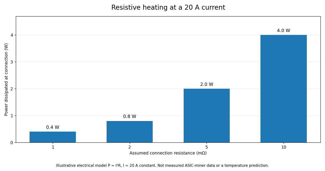
The formula alone does not predict component temperature. Temperature rise depends on thermal resistance, board copper, heat sinks, air or liquid cooling, contact geometry and time. It also does not prove that any observed discoloration arose from a bad solder joint. The practical value is recognizing why a small electrical-resistance change can matter at elevated current and why powered probing is not a routine classroom substitute for the approved test process.
Why Reflowing a Board Is Not the First Step
Adding heat before identifying the root cause can destroy evidence, shift fine-pitch components, damage laminate, alter metallurgical joints and contaminate nearby parts. Uncontrolled “whole-board reflow” is not a validated repair plan. Dense mining boards may have heat spreaders, soldered heatsinks and packages with concealed connections; repairing one visible defect does not verify the hidden ones. IPC also publishes dedicated rework/repair references such as IPC-7711/7721, which should be used with manufacturer controls and the specified equipment rather than guessed tip temperature or dwell time.
Adafruit Industries, “Collin’s Lab: Soldering,” April 10, 2014, accompanied by Adafruit’s free learning-system guide. Demonstrates wetting and practical workmanship fundamentals. Historical general-purpose teaching footage; not a current IPC inspection certification or mining-hashboard reflow recipe.
A rework authorization should identify the board model and revision, exact suspect joint, thermal limits of nearby components, approved solder alloy and flux, cleaning requirements, ESD protection, traceability and requalification plan. Some defects warrant board replacement or manufacturer return rather than component-level repair. In the cited S19k Pro support instructions, Bitmain explicitly differentiates acceptable return options for two constructions; never assume a third-party or an earlier miner has the same restrictions.
A Clear Accept, Rework, Replace, or Escalate Decision
- Accept for continued diagnostic review: no actionable visual defect found, and an authorized functional baseline is consistent with the expected model behavior. This is not proof that every hidden joint is sound.
- Request a closer inspection: discoloration, irregular appearance or ambiguous imaging without enough evidence to apply the specified standard. Record the ambiguity and avoid undocumented cosmetic rework.
- Hold for specialist rework review: a credible solder bridge, lifted land, fractured termination, local burning or other condition outside the approved inspection criteria. Preserve the original image and limit handling.
- Escalate to the manufacturer: inaccessible joints, uncontrolled thermal hardware, warranty or board-version restrictions, or any case where the repair method cannot be validated.
- Requalify only through an approved process: after an authorized repair, check for physical defects, appropriate electrical integrity, recognized board enumeration, correct temperature control and sustained performance as specified by the model’s service procedure.
Bitmain’s S19 low-hashrate troubleshooting document lists several causes for reduced performance, including dropped boards, frequency changes and unstable ASICs. Consequently, an apparently repaired joint should not be credited with fixing a complete machine solely because a brief hash test succeeds. Log correlation, thermal behavior and model-specific acceptance criteria are essential to a responsible release decision.
Documentation-Only Practical Lab
Learners can complete the practical activity using official photographs and a worksheet; no disassembly or soldering is required. Compare the two Bitmain S19k Pro images included above and identify the different heat-sink configurations. Explain which surfaces can be inspected without removing thermal hardware and why a photograph of an intact board is not evidence of a defect. Next, view the iFixit and Adafruit soldering demonstrations and write a short description of wetting versus bridging using the educational material, without attempting to classify hidden joints.
For a quantitative exercise, independently recalculate the 20 A model at 1, 2, 5 and 10 mΩ. Record the results as 0.4, 0.8, 2.0 and 4.0 W. Then explain why the chart cannot be used as a board temperature graph. Finally, prepare a mock service ticket with fields for miner model, board revision, reported symptoms, power-isolation evidence, photograph filename, visual observations, test references, escalation decision, and approval authority.
Knowledge Check with Answers
- Does a low ASIC count prove that one solder joint failed? No. Power delivery, signal routing, sensors, controllers, connector faults and silicon problems can create overlapping symptoms.
- Why does the exact S19k Pro board construction matter? Heat-sink configuration, substrate and service restrictions differ, changing what can be inspected and how a board may be repaired or returned.
- Is a dull lead-free solder joint automatically defective? No. Appearance alone is insufficient; compare applicable criteria and evidence.
- What is a solder bridge? An unintended electrical connection formed by solder between conductors that should remain isolated.
- Can a standard optical microscope prove concealed ASIC balls are intact? No. Hidden joints may require qualified nondestructive evaluation or other validated tests.
- What is the calculated power at 20 A through 5 mΩ? 2.0 W from P = (20 A)² × 0.005 Ω.
- Does a repaired miner passing a brief startup prove all joint reliability questions are resolved? No. Approved requalification and operating evidence are required.
- What is the preferred action when uncertain about a board’s rework method? Record the evidence and escalate to an authorized, trained repair process instead of applying uncontrolled heat.
Educational and Primary References
Manufacturer evidence: BITMAIN S19k Pro board identification and repair precautions; BITMAIN S19 board version identification; and BITMAIN low-hashrate troubleshooting. Educational inspection sources: NASA Workmanship Standards, IPC’s Introduction to IPC-A-610 syllabus, iFixit’s open soldering hub, and Adafruit’s Guide to Excellent Soldering. Verify the latest manufacturer and standards revisions before professional inspection or rework.
In the next curriculum rotation, the subject advances to a verified robotics technician lesson, rather than repeating hashboard inspection. The core principle from OSHRE.006 is that an observed surface condition is not a diagnosis until device identity, defect criteria and functional evidence support the same conclusion.
Editor’s Note: The S19k Pro photographs are genuine BITMAIN Support images, each attributed to its originating support bulletin. The featured 1200 × 630 cover is original AI-generated conceptual editorial artwork, not a documentary photograph of a specific miner. The chart is an original calculation using hypothetical resistance values, not measured operating data. Both videos are general educational demonstrations by iFixit and Adafruit; neither is a BITMAIN-certified rework method. No hashboard was disassembled, energized, soldered or repaired for this lesson. WordPress rendering, video playback and mobile layout checks are reported separately in the publication audit.
Mobile users can scan the original QR on a second screen with a compatible Bitcoin wallet, or import a saved image if the wallet supports QR scanning from images. Verify the receiving address and requested 5,000 sats before sending.
We volunteer daily to ensure the information on this platform is Verifiably True. If you would like to support the research, please scan the QR code.
BitcoinVersus.tech reports on financial and technical subjects for informational and educational purposes; the lesson is not an authorized live-electrical or manufacturer-repair procedure.


Leave a Reply