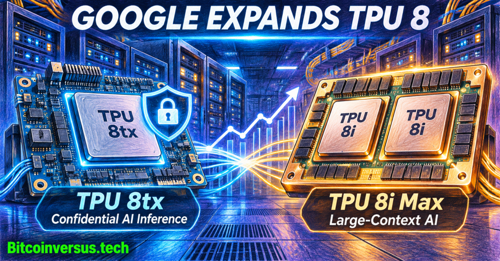
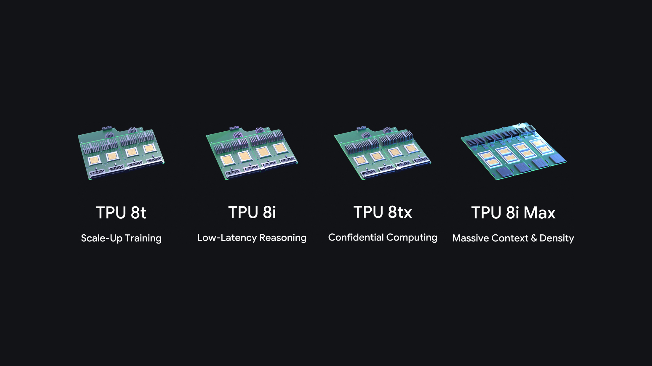
Google announced two additional eighth-generation Tensor Processing Unit (TPU) systems on November 9, 2026: TPU 8tx, designed for confidential AI inference, and TPU 8i Max, which combines two TPU 8i chips in one package. The additions expand the family to four systems, but they do not represent four independently designed new chips. The engineering story is how packaging, memory, networking and security can change accelerator behavior without requiring an entirely new silicon design.
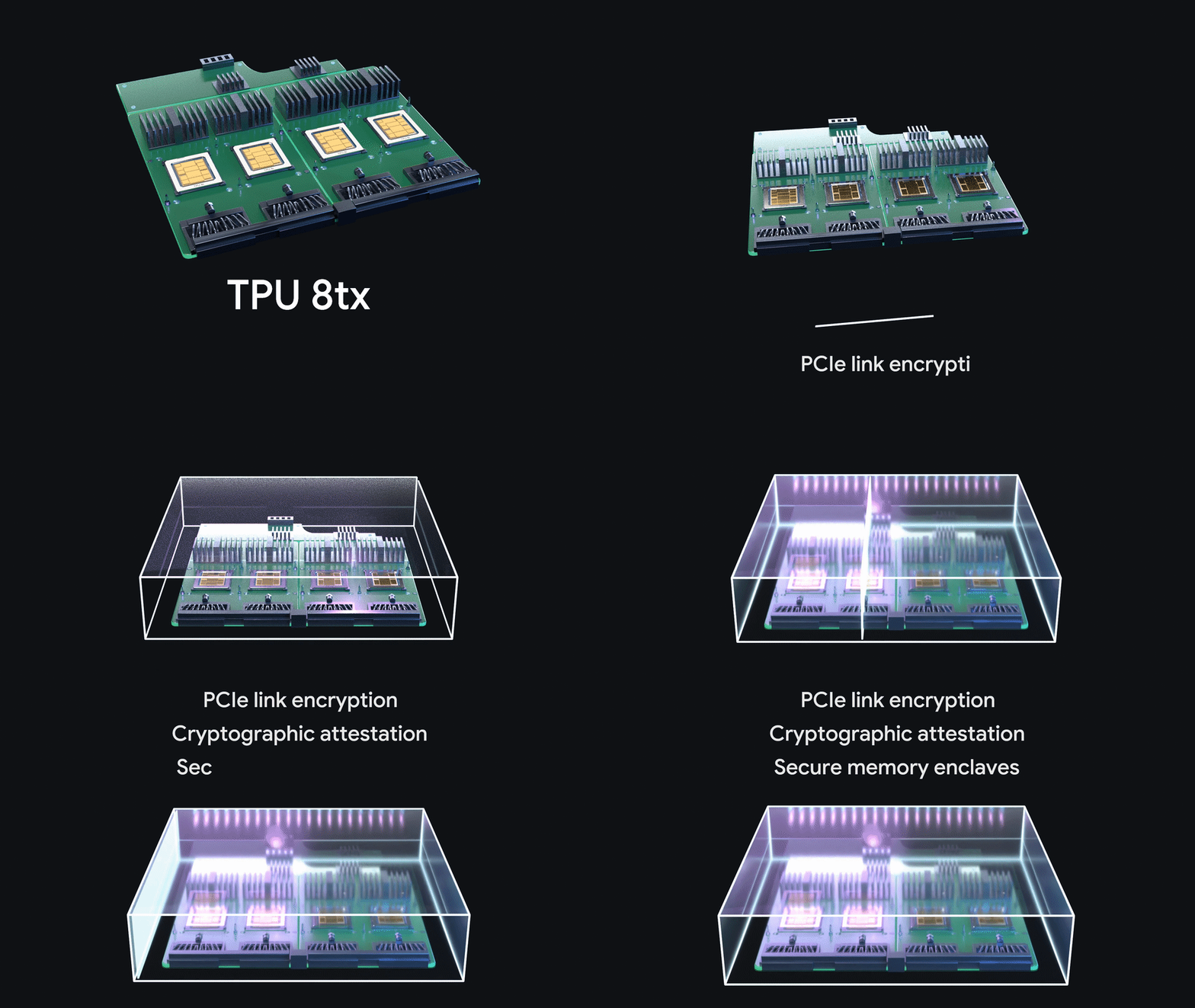
Confidential computing becomes a hardware feature
TPU 8tx reuses the silicon behind the training-oriented TPU 8t, pairs it with custom AMD CPU hosts and adopts Google’s low-latency Boardfly network. Google says hardware-level protections isolate sensitive model weights and data during active processing, rather than protecting information only while stored or in transit. The intended customers include regulated organizations that must process private information while running inference or fine-tuning models.
Google claims up to twice as low latency as TPU 8t, with a near-zero performance penalty from the security design. “Up to” describes a favorable measured condition, not a guarantee for every model, prompt or cluster. Independent confidential-computing audits, documented threat models and reproducible benchmark settings would be needed to establish how broadly the claim applies.
Two chips target the memory bottleneck
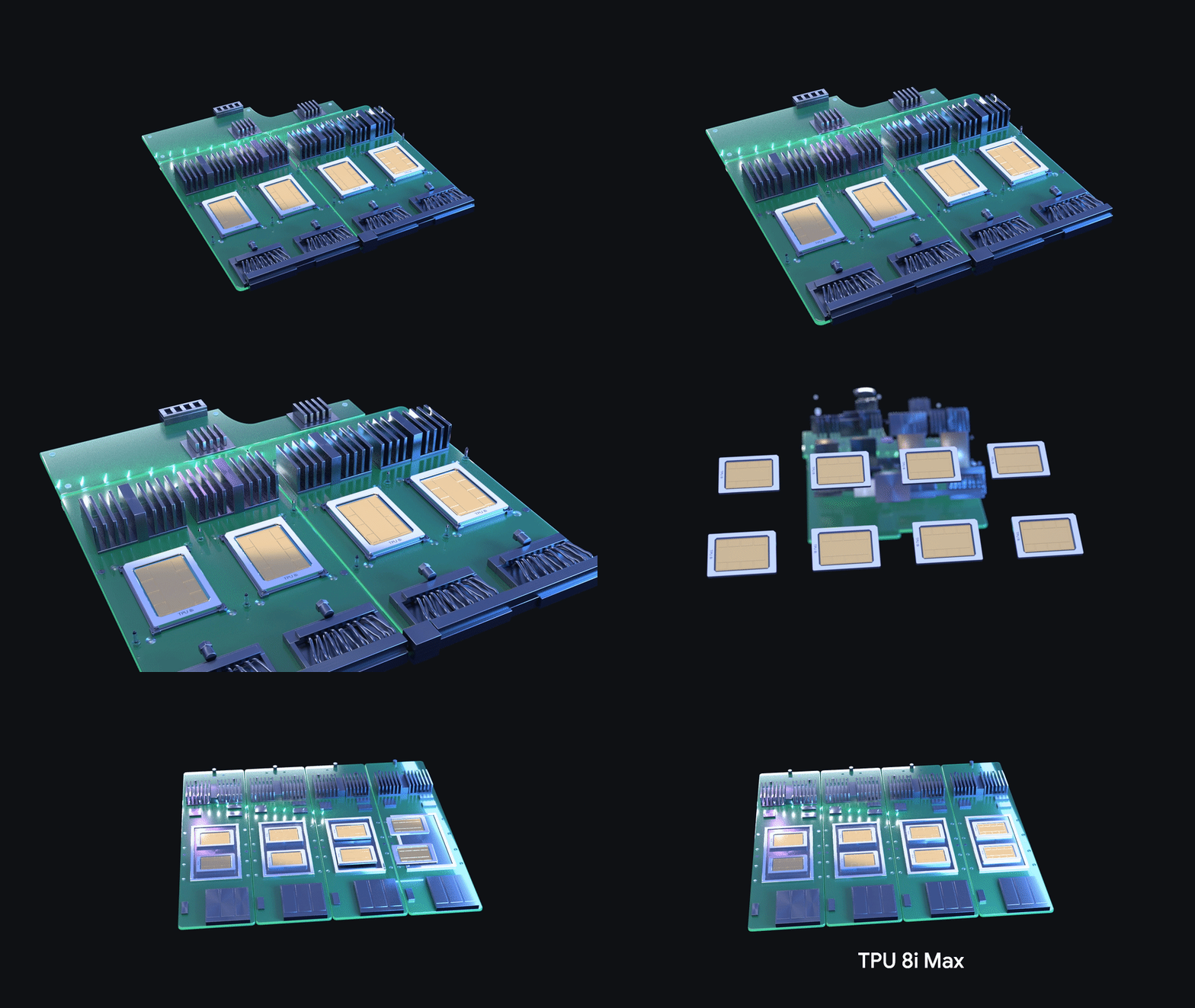
TPU 8i Max combines two TPU 8i chips inside one package. Google reports twice the compute capacity, on-chip SRAM and high-bandwidth-memory throughput relative to a single TPU 8i. Using Google’s previously disclosed 384 MB of SRAM per TPU 8i as a reference, the combined design implies approximately 768 MB of on-chip SRAM. The same arithmetic applied to the earlier 288 GB HBM capacity yields 576 GB, assuming memory capacity scales with the paired chips; Google’s November statement explicitly doubles HBM bandwidth, not necessarily every published capacity metric.
The important distinction is between a 100% increase in hardware resources and a 100% increase in completed AI work. Real throughput depends on inter-chip transfers, software scheduling, model size, memory access patterns and power limits. Google says the dual-chip configuration increases computing density within the existing rack footprint, but it has not provided enough public, workload-matched power and cost measurements to establish a universal tokens-per-watt advantage.
The software and network are part of the performance claim
Google also introduced TPU Sync, an open-source model-state layer connecting accelerator HBM, host memory, storage and the data-center network. Its published tests report more than 90% lower key-value-cache transfer latency and about 90% lower time to first token for specified large mixture-of-experts serving workloads. A 90% reduction means a process taking 100 milliseconds would take approximately 10 milliseconds under otherwise equivalent conditions; it does not mean every end-user response becomes ten times faster.
Separately, Google says dynamic slicing on Google Kubernetes Engine can cut job startup time by up to a factor of five and improve recovery by up to 4.5 times compared with static TPU slice provisioning. Those are infrastructure-management comparisons, not new chip-speed measurements. The developments extend the software strategy covered in Google’s open-source XLA Serving Engine and the earlier TPU software and Oracle expansion.
What remains to be demonstrated
The announcement strengthens Google’s position in AI infrastructure, following its reported cloud revenue growth and a TPU deployment plan at Purdue University. However, Google’s claims remain vendor-reported, and no like-for-like independent comparison against contemporary Nvidia or AMD accelerator clusters is established by the launch materials. Availability, pricing, measured electricity consumption and performance under independently selected models will determine the practical advantage.
Primary sources and methodology
Sources: Google’s November 9 TPU 8tx and TPU 8i Max announcement; Google’s TPU Sync technical announcement; Google’s dynamic slicing announcement; Google’s earlier TPU 8i specifications. Percentage and resource comparisons are manufacturer statements unless identified as arithmetic derived from published specifications.
Editor’s Note — November 10, 2026: The new systems are configurations based on existing eighth-generation TPU silicon, not two newly fabricated chip architectures. The featured cover is original conceptual artwork, not a photograph of actual hardware. The three in-story visuals are distinct Google-supplied product illustrations or animations. Vendor performance figures have not been independently reproduced. We volunteer daily to ensure information published on our platform is Verifiably True.
Support independent research
An optional 5,000-satoshi contribution can support ongoing research. Scan the QR code on a second screen or use a compatible wallet’s saved-image scanner on mobile. Verify the recipient address 3C9o19EH5HSiwEPyCTmEKzxhNCbo2X6TTb and amount before paying.

BitcoinVersus.Tech provides technology and financial reporting for informational purposes only and is not a financial adviser.


Leave a Reply