Siemens and TSMC are pushing agentic AI deeper into semiconductor engineering with a workflow that can automatically detect and correct physical chip design-rule violations instead of stopping at diagnosis.
The September collaboration combines Siemens’ Calibre physical-verification platform, Aprisa place-and-route technology and Solido simulation and design-environment tools with TSMC process technology. The result is an AI-assisted loop aimed at reducing one of the most repetitive and time-consuming stages of advanced-chip implementation.
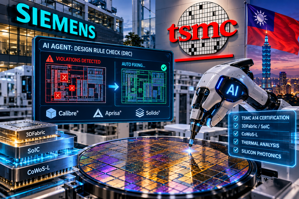
AI moves from finding errors to fixing them
The companies say an AI agent can identify design-rule-check violations, reason about potential corrections and drive automated fixes through the implementation flow. That is a meaningful step beyond simply using machine learning to rank warnings or optimize isolated design parameters.
Physical verification is unforgiving. A modern layout must satisfy foundry rules governing spacing, width, density, connectivity and manufacturing constraints across enormous numbers of geometries. At advanced nodes, correcting one violation can create another, forcing engineering teams through repeated implementation and verification cycles.
TSMC A14 joins the certified flow
The collaboration extends Siemens’ digital implementation and verification support to TSMC’s A14 process. That puts Siemens beside other EDA vendors advancing AI-assisted A14 workflows, including the Synopsys and TSMC agentic-AI work BitcoinVersus.tech recently covered.
The broader semiconductor race is increasingly about more than transistor scaling. Our recent reporting has followed High-NA EUV moving toward production, 2 nm connectivity silicon, and higher-density AI server memory. Automated design closure is another lever for turning those manufacturing capabilities into working products.
3DFabric, SoIC and CoWoS-L expand the problem
Industry coverage says the partnership also advances support for TSMC 3DFabric technologies, including SoIC and CoWoS-L, alongside thermal analysis and silicon-photonics design.
Those packaging systems matter because modern AI accelerators are increasingly assembled as systems of compute dies, HBM stacks, interposers and high-speed I/O rather than as a single monolithic chip. BitcoinVersus.tech has been tracking that trend through CXL memory expansion, optical-chip manufacturing expansion and rack-scale AI interconnect development.
Why automated DRC repair matters
A design-rule violation is not merely a software warning. It can represent geometry that a fabrication process cannot reliably manufacture. Automating the repair loop therefore attacks engineering iteration time directly: find the violation, understand its local layout context, alter the geometry, rerun verification and continue until the design closes.
Siemens is positioning agentic automation as a way to compress that cycle while engineers retain responsibility for the final design. The practical test will be how reliably an autonomous agent can make localized corrections without degrading timing, power, signal integrity or creating new violations elsewhere.
The same pressure is visible throughout AI hardware. Faster accelerators require increasingly sophisticated manufacturing, memory and packaging, while design teams must keep schedules under control. That is why EDA automation is becoming as strategically important as the lithography equipment and fabs that eventually manufacture the silicon.
BitcoinVersus.Tech Editor’s Note: AI-assisted EDA can automate portions of physical design and verification, but foundry certification and automated repair do not eliminate engineering signoff or guarantee that every design closes without manual intervention.
Support independent semiconductor, AI hardware and infrastructure reporting: 3C9o19EH5HSiwEPyCTmEKzxhNCbo2X6TTb
BitcoinVersus.tech is not a financial advisor. This media platform reports on financial subjects purely for informational purposes.


Leave a Reply