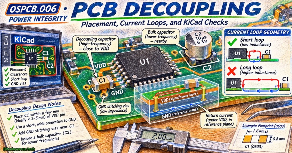
OSPCB.006 continues the Open Source PCB curriculum with a practical power-integrity problem: where should the capacitors around an integrated circuit go? Decoupling capacitors deliver short bursts of charge and provide a local return route for high-frequency switching current. Correct component values matter, but PCB trace geometry, nearby reference planes, vias and capacitor parasitics may determine whether a design actually works.
Texas Instruments Precision Labs: “Mixed signals, grounding and bypass capacitors,” April 14, 2021. Official vendor training addressing supply bypassing and grounding, not a test of the example board. Credit: Texas Instruments / YouTube.
Elementary overview and prerequisites
Think of a nearby ceramic capacitor as a small, fast energy reservoir placed beside an IC. During a switching event, the IC can draw current through a small local loop instead of depending entirely on a distant supply trace. The previous OSPCB.005 ground-plane lesson explained how return currents follow low-impedance paths. Also review PCB stackups and vias and through-holes.
Learning objectives: identify local and bulk capacitors, trace the complete switching-current loop, check DC-bias derating, estimate ideal voltage droop and inductive noise, then review a KiCad 10 PCB layout without mistaking DRC for electrical validation.
The complete current loop matters more than a ruler
A typical decoupling path runs from the capacitor’s positive pad to an IC supply pin and returns through the ground connection to the capacitor. Long traces and separated power/ground vias increase the potential loop inductance. A short local connection and a continuous adjacent reference plane can reduce it. For some multilayer plane-fed BGA designs, capacitor proximity is less decisive than plane spacing and via geometry; device-specific manufacturer guidance takes priority over fixed distance rules.
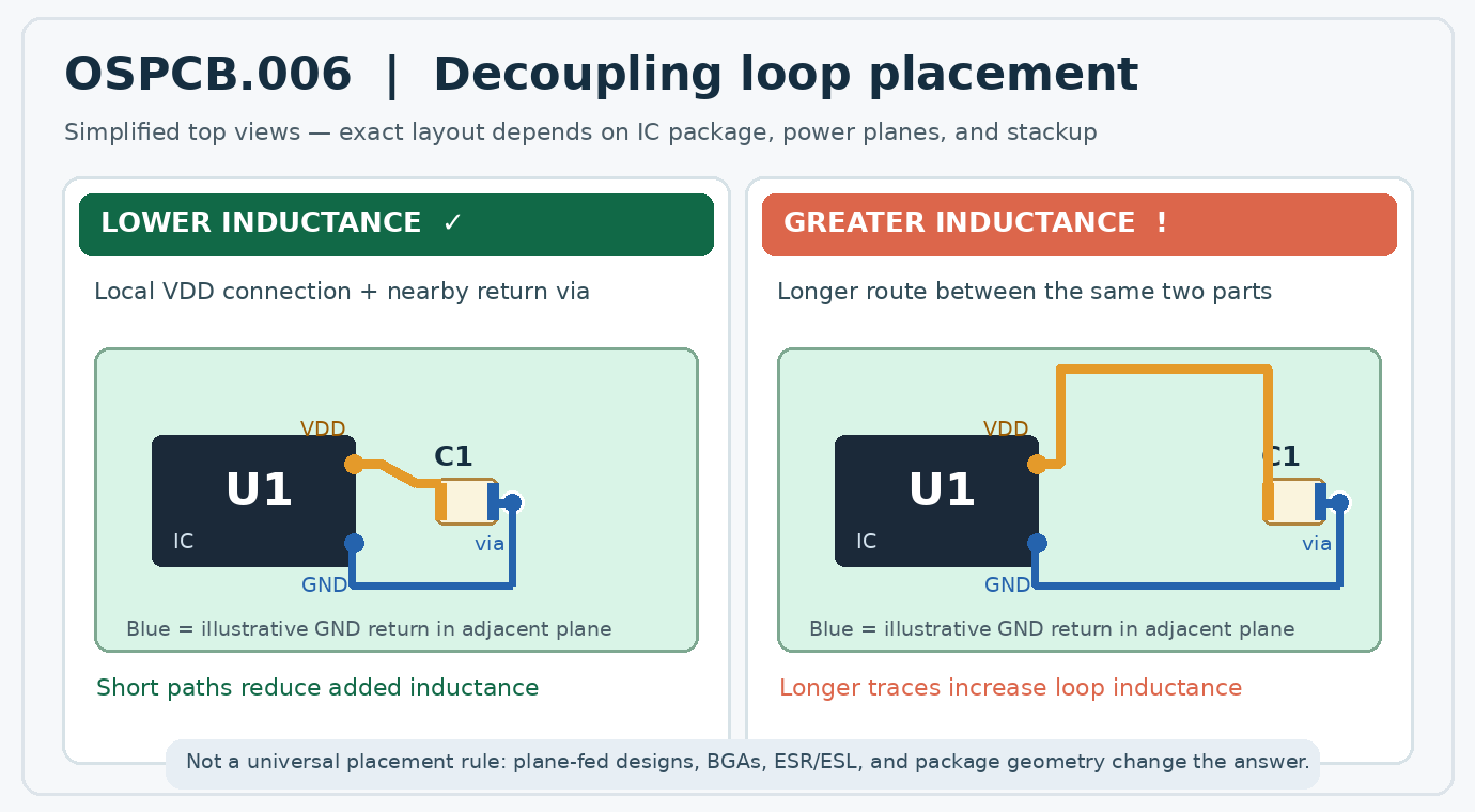
Worked example: capacitance versus inductance
Suppose a hypothetical IC requests an extra 0.20 A for 2 nanoseconds. An ideal 100 nF capacitor would lose only 4 mV, from ΔV = I × Δt / C. But an assumed 2 nH series inductance carrying a 0.20 A rise over 2 ns can produce 0.20 V from V = L × ΔI / Δt. Neither calculated value is a complete circuit prediction: voltage waveforms depend on package inductance, frequency, ESR, real capacitance, planes and other components.
A nominal 100 nF X7R ceramic may deliver less effective capacitance under DC bias. Larger bulk capacitors support slower load changes, while low-inductance ceramic parts address faster transients. Mixing capacitor values is not automatically better: resonance and antiresonance can create impedance peaks. Select values, packages and voltage ratings from the IC and capacitor manufacturers’ specifications.
Altium Academy, “Does Decoupling Capacitor Placement Actually Matter?”, April 9, 2026. Zach Peterson discusses why stackup and component packages affect placement decisions. Credit: Altium Academy / YouTube.
KiCad 10 practice workflow
- Open a non-energized training project and identify every IC supply/ground pin pair in the schematic.
- Assign the recommended bypass components and confirm voltage ratings, footprints and reference designators.
- In PCB Editor, place local capacitors according to the datasheet and inspect both sides of their current loop.
- Keep critical power/ground connections short; position ground vias according to the actual stackup and package.
- Refill all copper zones with B and inspect reference-plane continuity.
- Run Inspect → Design Rules Checker, including schematic parity where available. Review unconnected pads and clearances.
- Document any remaining power-integrity questions for manufacturer review, simulation or properly equipped lab testing.
Compare the workflow with OSPCB.004 routing and DRC and OSPCB.003 footprints. A passing DRC checks configured geometry and connectivity; it does not certify transient response, EMI compliance, capacitance under bias or acceptable solder assembly.
Knowledge check and conclusion
Question: Why can a longer bypass trace cause more noise despite having the same capacitor value? Answer: Added series inductance raises the voltage associated with fast current changes. Question: Does a KiCad DRC pass prove low impedance? Answer: No; DRC does not replace electrical characterization.
A reliable decoupling design begins with the complete current loop. Choose capacitors for the intended frequency range and operating bias, apply the actual device layout recommendations, then verify connections and the board stackup before manufacturing.
Primary sources and calculations: Analog Devices, mixed-signal PCB layout and decoupling guidelines; Analog Devices, minimizing ESR/ESL in power-converter loops; KiCad 10 official PCB Editor documentation; TDK, DC-bias behavior of multilayer ceramic capacitors; Analog Devices capacitor self-resonance and frequency selection; Texas Instruments Precision Labs video; Altium Academy decoupling placement video. Example arithmetic: (0.20 A × 2 × 10−9 s) / (100 × 10−9 F) = 0.004 V; (2 × 10⁻⁹ H) × [(0.20 A) / (2 × 10⁻⁹ s)] = 0.20 V. Both component values and waveforms are illustrative.
Editor’s Note: OSPCB.006 follows the previously published OSPCB.005 chapter on ground planes. Technical explanations are based on primary manufacturer documentation and KiCad 10 references. The 4 mV ideal-capacitance and 0.20 V ideal-inductance results are separate hypothetical calculations, not a verified physical PCB voltage waveform. The original 1200 × 630 cover is colored-pencil conceptual artwork with a neon-green 10-point bottom-left Bitcoinversus.tech watermark; the in-story current-loop diagram is original and not a field-solver result. Both educational videos were identified by title, channel and public watch ID. No KiCad project was opened, no board was manufactured or measured, and public video playback and mobile layout were not independently tested at drafting.

BitcoinVersus.Tech is volunteer-run and publishes independent technical education. An optional 5,000-satoshi donation supports ongoing research. Scan the original QR from a second screen with a compatible Bitcoin wallet. On the same phone, use a wallet that can read a saved QR image if supported. Independently verify the recipient address 3C9o19EH5HSiwEPyCTmEKzxhNCbo2X6TTb and the amount before sending; Bitcoin transfers are generally irreversible.
We volunteer daily to ensure the information on BitcoinVersus.Tech is Verifiably True. Coverage is educational and informational and does not constitute individual electrical engineering certification, manufacturing approval, financial or investment advice.


Leave a Reply