Photoresist is the light-sensitive coating that lets chipmakers transfer microscopic circuit patterns onto a silicon wafer. It is one of the most important materials in photolithography: coat the wafer, expose selected areas to light, develop the resist, and the resulting pattern becomes a temporary stencil for the next manufacturing step.
The basic idea sounds almost like photography, but the scale is radically different. Modern semiconductor fabs use photoresist to define structures measured in nanometers, repeating the process layer after layer until billions of transistors and their interconnects have been built across a wafer.
Photoresist Is a Temporary Patterning Layer
Samsung Semiconductor describes photoresist as a photosensitive material that changes chemically when exposed to light. That controlled chemical change is what lets the fab create a pattern on the wafer instead of modifying the entire surface at once.
Think of the resist as a temporary protective stencil. Some areas remain covered after development while other areas are opened. The exposed underlying material can then be etched, implanted, deposited on, or otherwise processed. After that step is complete, the resist is stripped away and a new pattern can be created for another layer.
Step 1: Coat the Wafer
The process begins with a clean wafer surface. A small amount of liquid photoresist is placed near the center of the wafer and the wafer is spun rapidly. Centrifugal force spreads the liquid into a very thin, uniform film.
Uniformity matters because the lithography system is trying to focus an extremely precise image onto that surface. Thickness variation, particles, bubbles, contamination, or poor adhesion can distort the pattern and eventually hurt wafer yield.
OSHA’s semiconductor fabrication guidance describes this same spin-coating method: liquid resist is delivered to the center of the wafer and high-speed rotation spreads it across the surface as a thin coating.
Step 2: Bake the Resist
After coating, the wafer usually receives a controlled bake. This removes solvent, stabilizes the resist film, and prepares it for exposure. Semiconductor patterning is full of these seemingly small process steps because material chemistry has to remain extremely repeatable from wafer to wafer.
The resist is not simply paint sitting on silicon. Its thickness, solvent content, adhesion, chemical composition, and sensitivity all influence how faithfully the lithography system can reproduce the intended geometry.
Step 3: Project the Circuit Pattern With Light
This is where ASML lithography systems enter the process. ASML describes lithography as a projection system: light passes through or reflects from a patterned mask or reticle, and precision optics shrink and focus that pattern onto the photosensitive wafer.
The wafer stage then moves and the scanner repeats the exposure across the wafer. The same idea connects directly to the photomask and High-NA EUV problems BitcoinVersus.Tech has covered: the mask contains the pattern, the optics project it, and the resist is the material that records where the light landed.
ASML’s lithography guide says an entire microchip can require the patterning cycle to be repeated 100 times or more as one layer is aligned on top of another.
Positive vs. Negative Photoresist
Photoresists can respond to exposure in two broad ways. With a positive photoresist, the exposed areas become easier to dissolve during development, so those exposed regions are removed. With a negative photoresist, exposure causes the illuminated regions to remain while the unexposed regions are removed.
SK hynix explains that positive resist is commonly favored for very fine semiconductor patterns, while negative resist can offer advantages such as stronger resistance during later processing. The right chemistry depends on the layer, resolution target, and downstream process.
Step 4: Develop the Pattern
After exposure, the wafer goes through development. A chemical developer selectively removes the soluble portions of the resist. What remains is the physical resist pattern that protects some areas of the wafer while leaving others open.
Samsung compares this step to developing a photograph: the exposure is converted into a visible physical pattern. In semiconductor manufacturing, however, that pattern is not the finished product. It is the template for what happens next.
Step 5: Etch, Deposit, or Modify the Open Areas
Once the resist pattern is developed, the fab can selectively process the exposed material underneath. An etch step can remove material. An ion-implantation step can introduce dopants. A deposition process can add material in selected regions or prepare the wafer for later pattern transfer.
This is why lithography and deposition are tightly connected. BitcoinVersus.Tech recently covered how ASM is pushing atomic-scale deposition as transistor structures become more three-dimensional and harder to manufacture. The resist tells the fab where a process should act; tools for deposition, etch, implantation, and cleaning determine what happens there.
Why Cleanrooms Use Yellow or Orange Light
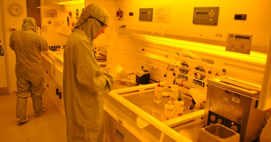
Many photolithography areas are intentionally lit with yellow or orange light. That is not just atmosphere. The room lighting is selected to avoid wavelengths that could unintentionally expose light-sensitive resist before the wafer reaches the lithography tool.
The featured photograph for this article comes from a University College London photolithography cleanroom whose orange lighting is specifically used to protect photoresist from damaging short-wavelength ambient light.
DUV and EUV Need Different Resist Chemistry
Photoresist has had to evolve alongside lithography light sources. Older and less demanding layers can use visible, i-line, KrF, or ArF resist systems. Leading-edge layers can require resist chemistry engineered for extreme ultraviolet, or EUV, exposure.
Fujifilm Electronic Materials lists photoresist families spanning i-line, 248 nm KrF, 193 nm ArF, e-beam, and EUV applications. That range shows why “photoresist” is a material category rather than one universal chemical formula.
The wavelength matters because shorter-wavelength systems can print smaller features. ASML’s light-and-lasers documentation explains the progression from older mercury-line systems to 193 nm DUV and finally 13.5 nm EUV.
EUV Photoresist Is Becoming Its Own Technology Race
At advanced nodes, the resist itself becomes part of the scaling challenge. The material must be sensitive enough to expose efficiently, stable enough to produce repeatable patterns, and capable of resolving extremely small features without excessive roughness or random defects.
JSR has been expanding development and production around metal oxide resist, or MOR, for EUV. In 2026, JSR’s Inpria and Entegris also announced a cross-license covering metal-oxide-resist patents for next-generation EUV lithography.
That materials race sits directly alongside the hardware race in High-NA EUV. Better optics alone are not enough if the resist cannot faithfully record the smaller image being projected onto the wafer.
Why Photoresist Defects Hurt Yield
A particle, bubble, thickness error, incomplete development, chemical contamination, or random resist defect can distort a feature. If that feature belongs to a transistor gate, contact, or interconnect, the resulting die may fail electrical testing.
That is why resist quality eventually shows up in the economics of good dies per wafer. The fab is not paid for drawing beautiful patterns; it is paid for producing working chips. Pattern fidelity, defectivity, overlay accuracy, etch quality, deposition control, and inspection all contribute to that final yield.
Photoresist Comes Before Packaging
Photoresist is mainly part of the front-end wafer fabrication process. The wafer is patterned repeatedly until the transistor and interconnect structures are complete. Only later are individual dies tested, cut, and moved into semiconductor packaging.
That distinction matters because the finished CPU, GPU, memory device, ASIC, or sensor has already passed through many photoresist cycles before it ever reaches a package substrate, solder joint, heat spreader, or circuit board.
The Simple Way to Remember It
Photoresist is the wafer’s temporary light-sensitive stencil. Coat it. Expose it through a pattern. Develop it. Process the open areas. Strip it. Then repeat for the next layer.
The 300 mm wafer provides the manufacturing surface. The photomask carries the pattern. The lithography tool projects it. Photoresist records it. Etch and deposition tools turn that temporary pattern into permanent semiconductor structures.
Editor’s Note
Photoresist formulations, bake temperatures, exposure doses, developer chemistry, film thicknesses, and process sequences vary by fab, lithography wavelength, device layer, and manufacturer. This article describes the general photolithography flow rather than a specific proprietary semiconductor process recipe.
Featured image: photolithography laboratory in the London Centre for Nanotechnology cleanroom, University College London Faculty of Mathematical & Physical Sciences, via Wikimedia Commons; cropped to 1200×630 for BitcoinVersus.Tech.
Support and donation options are available through BitcoinVersus.Tech.
BitcoinVersus.tech is not a financial advisor. Content is provided for informational purposes.


Leave a comment