One of the biggest bottlenecks in AI chips is moving closer to U.S. soil. GlobalFoundries announced a $2 billion, five-year manufacturing agreement with TSMC to produce silicon interposers at its Malta, New York facility for TSMC’s CoWoS advanced-packaging ecosystem.
Reuters reports that volume production is expected to begin ramping in the first half of 2028. GlobalFoundries says the expansion is designed to create the first U.S.-based source of silicon interposers supporting advanced AI packaging and gives both companies a framework to add more capacity if demand keeps growing.
What Is a Silicon Interposer?
A silicon interposer is a large piece of silicon that sits beneath multiple semiconductor dies and provides extremely dense electrical connections between them. In an AI package, that can mean linking a large GPU or accelerator to several stacks of high-bandwidth memory while keeping signal paths short enough to support enormous data rates.
The interposer is not the main compute die, but it can determine whether the processor and memory can communicate fast enough to behave like one high-performance system. That is why advanced chip packaging has become as strategically important as the transistor process itself.
CoWoS Is the Packaging System Behind Many AI Accelerators
TSMC’s CoWoS, short for Chip-on-Wafer-on-Substrate, is one of the core packaging technologies behind modern AI systems. A large logic die is placed beside HBM stacks on an interposer or related redistribution structure, and that assembly is then attached to a package substrate.
The package effectively turns several separate pieces of silicon into one tightly connected compute module. BitcoinVersus.Tech has already followed how HBM demand is pulling on the broader memory market and how packaging capacity has become a constraint on how quickly AI accelerators can ship.
WIRED highlighted the same industry shift earlier in 2026: advanced packaging has moved from a back-end afterthought to one of the central technologies shaping the AI boom.
GlobalFoundries Will Build the Interposers in Malta, New York
Under the agreement, GlobalFoundries will add manufacturing capacity at its Malta facility in New York. The company says the expansion will support silicon interposers used in TSMC’s CoWoS ecosystem and include capabilities such as embedded deep-trench capacitor components.
GlobalFoundries already operates advanced-packaging capabilities in the United States and Singapore. Its advanced-packaging portfolio includes 2.5D and 3D integration, interposers, wafer-to-wafer bonding, die-to-wafer bonding, through-silicon vias, assembly, and test.
Why TSMC Needs Another Interposer Supplier
The AI boom is putting pressure on nearly every layer of the semiconductor supply chain. TSMC can manufacture leading-edge logic dies, but an accelerator still needs HBM, interposers, substrates, assembly, test, power delivery, and cooling before it becomes usable hardware.
Reuters says advanced packaging remains a major constraint because demand has outrun available capacity. Adding GlobalFoundries as a U.S. manufacturing source gives TSMC another place to produce one of the most important physical components inside the package.
Reuters reported in July that TSMC was adding two more advanced-packaging plants in Taiwan, illustrating how aggressively the company has been expanding this part of the supply chain.
The Deal Connects AI Logic and HBM
The most visible components inside an AI accelerator are usually the GPU and the HBM stacks, but the interposer is what allows those components to exchange data across thousands of high-density connections.
That relationship helps explain why memory companies such as SK hynix, Micron, and Samsung are tied directly to the packaging bottleneck. Producing more HBM does not help if there is not enough packaging capacity to connect it to AI processors.
Through-Silicon Vias Move Signals Through the Interposer
Advanced interposers can use through-silicon vias, or TSVs, to move electrical connections vertically through silicon. Those vertical paths help connect dies mounted above the interposer to the package substrate below while allowing extremely dense routing between processors and memory.
TSVs are one reason the interposer itself requires semiconductor-style manufacturing. It is not simply a printed circuit board. It goes through wafer-level processes involving deposition, lithography, etching, metal routing, passivation, and precision alignment.
Interposer Manufacturing Still Depends on Fab Fundamentals
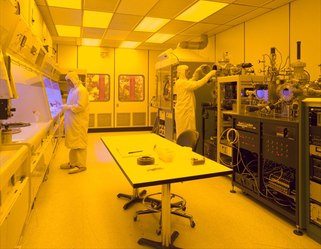
The same contamination controls that define a semiconductor fab cleanroom matter here too. Particles, alignment errors, defects, and process variation can reduce yield across a large interposer wafer.
Manufacturing also depends on familiar wafer processes. Photolithography defines patterns, etching removes material, metal layers form interconnects, and the completed wafer is eventually diced and integrated into packages.
Large Interposers Make Yield and Cost Harder
AI packages are getting physically larger. More HBM stacks and larger accelerator dies require more interconnect area, pushing interposers toward sizes that can exceed the exposure field of a single lithography reticle.
That is why techniques such as stitching and CoWoS-L matter. BitcoinVersus.Tech previously covered how CoWoS-L pushes packaging beyond traditional reticle limits. Larger package footprints give designers more room for compute and memory, but they also make manufacturing, yield, warpage, power delivery, and thermal control harder.
This Is Also a U.S. Semiconductor-Supply-Chain Story
For years, U.S. semiconductor policy focused heavily on bringing leading-edge wafer fabrication back to domestic sites. The GlobalFoundries-TSMC agreement highlights a second problem: manufacturing the logic die is only one step in producing an AI accelerator.
Packaging, substrates, interposers, memory, testing, and assembly also need enough capacity. A domestic silicon-interposer source gives TSMC and its customers another U.S.-based manufacturing node inside that larger chain.
Volume Production Is Expected to Ramp in 2028
Reuters says volume production is expected to begin ramping in the first half of 2028. That timeline means the deal is aimed at the next generation of AI infrastructure rather than solving today’s packaging shortage immediately.
By then, AI systems are expected to use even more HBM, larger packages, faster optical links, and denser accelerator racks. Packaging capacity will have to scale alongside the memory, compute, and networking hardware around it.
What to Watch Next
The biggest questions are how much interposer capacity GlobalFoundries ultimately adds in Malta, which CoWoS generations will use the U.S.-made components, how quickly TSMC expands advanced packaging elsewhere, and whether packaging supply can keep pace with the next wave of HBM-heavy AI accelerators.
The strategic lesson is straightforward: the AI chip is no longer just the logic die. It is the processor, HBM, interposer, substrate, power delivery, cooling, and test flow working together as one system. TSMC’s decision to bring GlobalFoundries into that chain shows how valuable the once-overlooked silicon underneath the GPU has become.
Editor’s Note
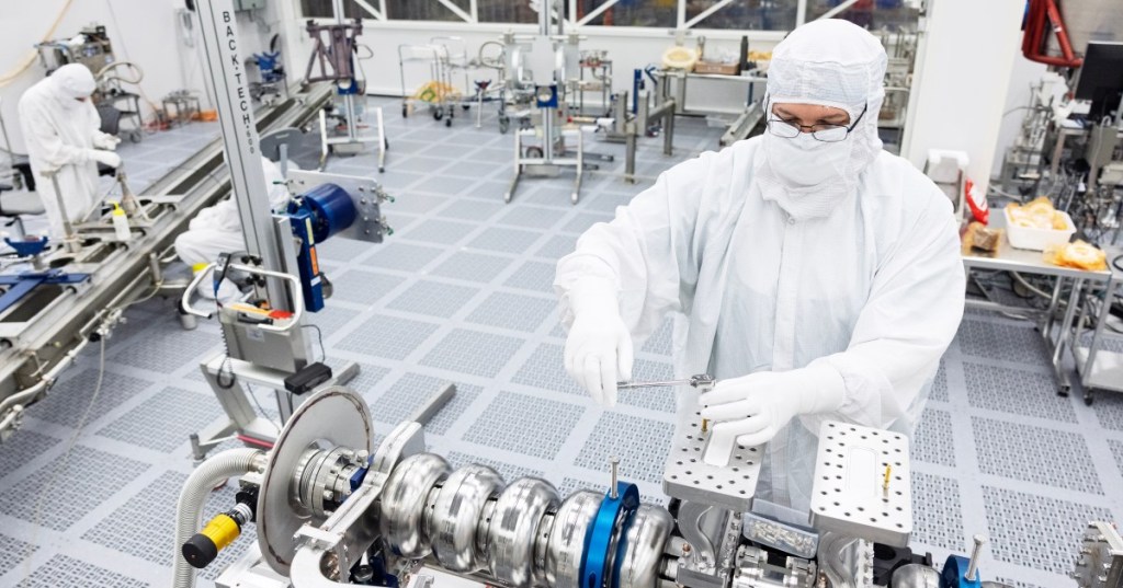
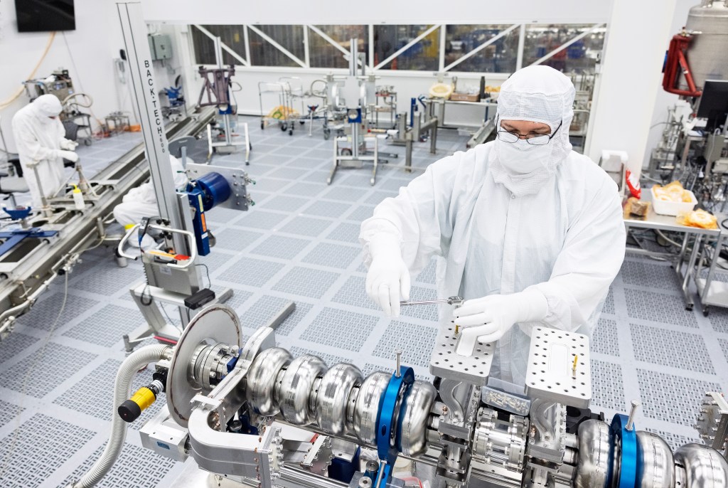
The agreement was announced October 8, 2026. Deal value, timing, and production plans are based on GlobalFoundries’ official announcement and Reuters reporting. Featured and body photographs are public-domain cleanroom images used to illustrate semiconductor manufacturing environments; they do not depict GlobalFoundries’ Malta line itself.
Support and donation options are available through BitcoinVersus.Tech.
BitcoinVersus.tech is not a financial advisor. Content is provided for informational purposes.


Leave a comment